Posted this at neo-geo.com too, but maybe someone on here can assist
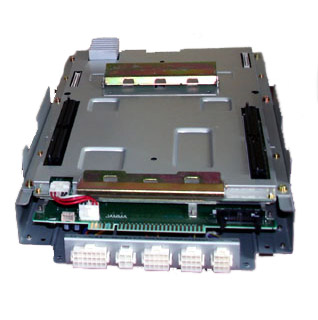
My driving I/O board JUST has two two JST two row connectors. One 32 pin, and one 34 pin.
The main front facing 21/4/15/12/9 larger connectors, whose wires go up into these 32/42 connectors, as well as all the associated wires were not included when I bought the I/O board.
Same config as Rev 2 fighting motherboards on the front, but I/O input connectors are totally different.
I color mapped the "potential" combinations to correctly hook up my wheel / pedals, from the 21 pin front facing connector to the dual row 34 pin connector off photos graciously taken by Suicidekiller over at NG.COM, and the combinations are too great to guess at. Were talking each potential ground having six places, 5V having 5+, etc etc.
Not to mention all the signal wires
I could guess all day and never get close. Statistically the probability sucks. I uploaded my possibilities of a pinout photo...and it's not pretty lol
So would anyone be willing to disconnect their driving board harnesses, and ship them to me so I can check them out? Or do an accurate pinout of the JST 21 pin connector, and where each wire goes exactly into the 34 pin connector pictured below
I'll buy you beer or pizza. Like seriously I'll toss you some cash to help me avoid this headache
Oh and I checked the schematics. They only show wires into the 21 pin front connector. They never show the CON4 34 pin connector TO the JST 21 pin harness on the front of the mobo
 lol
lol