What's new
Connect the pad to the regulators input and the regulators output to the new chip.
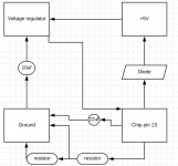
solid plan but it will be really tight to grab 5V from the pad, I'd recommend finding an easier location like a near-by filter cap.

the only other pin you need to be weary of is pin 33. on the original chip this changes it from 8-bit mode to 16-bit mode (low= 8bit, high=16 bit) and on the new chip it's write-enable pin (low=write mode, high=read mode). You'll want pin 33 tied high. presumable it should already be tied high to force the original chip into 16-bit mode but it's worth verifying. I suppose if it's not high then you'll have other issues since the new chip doesn't support 8-bit mode anyway. basically just use a multimeter and make sure this pin is already tied to 5V

you also mentioned pins 13/32 but these should be ground on both chips.

For the regulators I've used these with good success on a number of conversion/repairs: https://www.ebay.com/itm/2x-3-5-5V-...a=0&pg=2047675&_trksid=p2047675.c100005.m1851

there's no reason the ones you've specced out on Amazon shouldn't work though.
 
Last edited:
no problem, I can probe around and find a good +5v signal elsewhere if need be.

how can I make sure that pin 33 is tied high? I don't currently have a logic probe :/
 
just use that, you can test it with the board off and see if that pin has continuity to the 5V pin or any other 5V source.
 
cool, pins 23 and 33 have continuity, meaning that the write enable will always be tied high for read mode on the new chip, correct?
should I also lift pin 33 and tie it to the voltage regulator I will already be using?
 
so I've got the new chip installed, wiring up the voltage regulator.
I've got ground and +5v at the regulator, but nothing coming out.

per this data sheet- https://www.digchip.com/datasheets/parts/datasheet/015/AMS1117-pdf.php
I have ground going to pin 1, the voltage output going to chip pin 23, and +5v at pin 3.
I'm pulling +5v and ground from the connector used to connect to the motherboard.

However, I've got nothing coming off pin 2 of the voltage regulator.
Is the large tab opposite pins 1, 2, & 3 used for anything?
 
Is the large tab opposite pins 1, 2, & 3 used for anything?
the datasheet you linked says "TAB IS OUTPUT"

you might want to look at page 4 of the document you linked. there are additional resistors and capacitors necessary to make it function.
 
Okay, so looking at that I get this-

Need a 10uf non polar electrolytic capacitor between regulator pin 1 and ground
Need a resistor between the regulator's pins 1 and 2
Need a 22uf tantalum capacitor between pin 2 and ground
Need a diode between pins 2 and 3
Need another resistor from pin 2 to ground

My questions-
What kind of diode do I need? I read that it should be blocking voltage from running straight from pins 2 to 3, but allowing 3 to 2.
What resistor values do I need?
If I'm understanding this correctly, the resistor line should be tied to ground and is not a direct tie in any way to the chip on the cart.
 
Last edited:
Here's a visual of what I mean
 

Attachments

  • voltage regulator.png
    voltage regulator.png
    26.4 KB · Views: 124
You should really read the entirety of page 4.

According to the text in the spec sheet the diode is optional since it has an internal diode.

The resistor values change depending on the specific output voltage you want. there is an equation for calculating their value also on the spec sheet.

Avoiding these kinds of headaches are exactly why I buy the pre-built regulator circuits like the ones I linked earlier :P

here's a picture of one using the same regulaor you're using if you want to take notes on how they setup their circuit:
https://www.ebay.com/itm/5-PCS-DC-5...a=0&pg=2047675&_trksid=p2047675.c100005.m1851

s-l1600.jpg
 
Last edited:
A simple LDO regulator will be fine for 5v to 3.3v - that's what is generally used on the PGM conversions.
 
well I installed and verified the voltages, no dice :(
Any ideas?
 
the issue is unchanged, same graphical glitches as before
 
do you have a picture of your installation, are you sure everything is soldered well with no cold joints and no bridged joints?
do you have any pictures of the PCB area around your chip? was anything else damaged when the original Mask ROM burned a hole in itself?
do you have a picture of the check sum error, is it different than before?
 
Back
Top