Finisterre
Professional
I had thought this at one point as well. I'll try to get my Triforce out soon, wife is due on Friday with my second child, so time is limited!I had figured as much as I don't see why it would ever need direct access to nvram but one can be hopeful. Maybe the host options only work on triforce since that's where these commands came from but I don't have one to verify.
These articles seem to be from when the Triforce tools were first created:
"I’m sitting on this for a while now, and it didn’t change a lot. That means it’s either 100% finished or completely useless. It’s a python script which talks to the NetDIMM board on a Triforce/Naomi/Chihiro, and implements the “Satellite” protocol for uploading and running games"
https://debugmo.de/2009/04/triforce-tools/
It does appear from https://debugmo.de/2010/12/the-last-piece/ that we have indeed lost some info.
This forum post & forum are both gone for example https://assemblergames.com/forums/showpost.php?p=296558&postcount=7, or http://www.assemblergames.com/forum...Naomi-Security-Pic-Dumper&p=296558#post296558
It seems to be in the Internet Archive luckily:
https://web.archive.org/web/2013022...Naomi-Security-Pic-Dumper&p=296558#post296558
"By the way, the newer ("type 3") devices contain a nice new secret: They split out all the network/vxworks stuff into a MIPS cpu on a separate board. The GDROM-functionality and the PIC security now happens in the "RX850"-part - whatever that is. My closest guess: RX850 is a small RTOS from NEC for their V850 cpus, and the actual software running the GDROM-stack. The actual firmware isn't stored in a separate flash rom (there just isn't one left...), but uploaded from the SEGABOOT (the triforce-logo and testmenu thing which runs on the gamecube). My guess is that it's the firmware.asic file, a ~96k block-encrypted (DES?) file. I wasn't yet able to decrypt that mysterious data blob, but i'm pretty sure that it turns out to be the gdrom-stack / pic security. The SEGA part must then also contain the CPU - again, there is no other device left. Strange thing, isn't it?
...
As an interesting side note, the "netfirm" (the software running on the network board) has an open port, which you can use for a various amount of things, like:
- dumping the DIMM memory,
- read/write the *gamecube* memory (with help from SEGABOOT, so it's just part of the DI protocol spoken),
- read/write nvram, netfirm flash, set security keycode."
So there are indeed some documented differences in the Triforce version 3 at the very least per the above, and the following: https://debugmo.de/2008/08/triforce_type3/
"As a side note, the Netfirm can communicate with the gamecube software over specific DI commands (or, technically, answers: the gamecube constantly polls for queries from the DIMM board/netfirm). The Netfirm has a nice “debug-mode”/”development”/”backdoor” on tcp port 10703, which allows you to read/write gamcube memory (isn’t that nice?) as well as DIMM memory as well as the DES key for the uploaded content (as decryption happens on the fly)… … … Guess what we will see next."
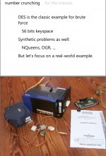
I didn't realize Felix Domke (tmbinc - https://twitter.com/tmbinc) was the father of all this research TBH. Parts of the talk "Distributed FPGA Number Crunching For The Masses" appear to be based on his work with Triforce.
https://events.ccc.de/congress/2010/Fahrplan/events/4203.en.html
https://events.ccc.de/congress/2010...uted FPGA Number Crunching for the Masses.pdf

"There is some "development mode" which might help here? (I think that one is activated if the PIC responds with a zero key. Not sure anymore, need to look at the disassembly again). Building a PIC with a zero key wouldn't be that complicated (some people can do that today
 ."
."does this mean we are technically running in development mode aka jumping into naoSetDevMode() when we use a zero key?
Here is the video for the talk Felix gave...
Worst case, perhaps Felix can answer some questions for us.

