What's new
Thanks @Apocalypse! Thanks @oneleaf86!

Personally I've already got DOJ, but I'm super excited to see this info find its way public. I'd tried offering up my carts to see this done a few times but no one wanted to take over the SMD side of things.

YOU GUYS ROCK!

I'm excited to see Espgaluda come around as that's the only one I've got left to obtain :).
 
Ketsui conversion on Knight of Valour 2:

I can't guarantee there's no mistake in the information given, I don't have any donor cart to do the conversion from scratch myself.
Also file names in the MAME romsets don't correspond to the donor used here so I've tried to figure this out.
The model cart being borrowed from @oneleaf86, I don't want to mess to much with it (i.e. desoldering chips and dumping them).

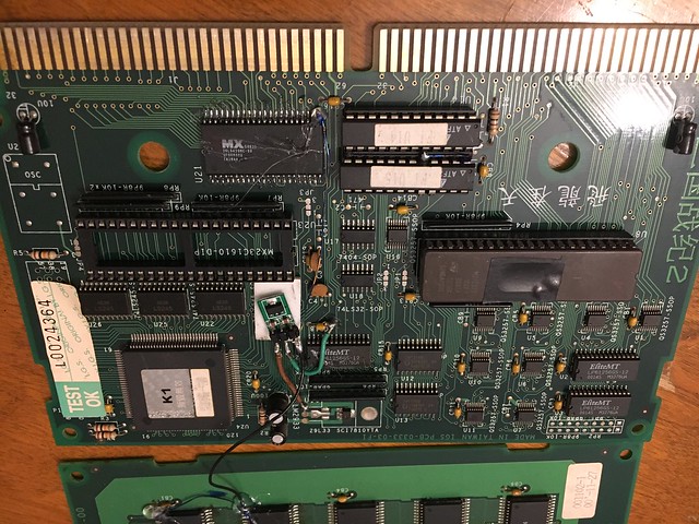
Donor PCBs look like this:


Link to the needed files:
http://www.filedropper.com/ket

Chips needed:
- 1 * 27C322 (can also use 27C160 if connecting pin 32 to Vcc)
- 4 * MX26L6420
- 1 * MX29L3211
- 1 * LDO 3.3V regulator (not sure how much current is needed, 500mA is probably more than enough)

Burn the files in the appropriate devices:
ketsui_u1.bin => 27C322 (U8)
t04701w064.u19 => MX26L6420 (U21)
a04701w064.u7 => MX26L6420 (U1)
a04702w064.u8 => MX26L6420 (U4)
b04701w064.u1 => MX26L6420 (U5)
m04701b032.u17 => MX29L3211 (U3)

Hardware mod:

PROG board:
1) Pull ROMs U8 & U21
2) Install new U8 and U21 but don't solder pin 23 of U21, lift it
3) Install 3.3V regulator (cart on the picture has a resistor and 2 diodes but I don't advise doing so)
4) Connect lifted pin of U21 to 3.3V from regulator
5) Bend legs 5, 20 & 21 of U15 so they stick out of the socket
6) Connect pin 5 of U15 to +5V (can be found in many places including upper via of CB12). Pins 20 & 21 are left unconnected.


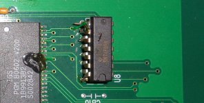
7) Connect pin 6 of U15 to pin 20 of U15 on the solder side (see picture below)
8 ) If using a 27C322 for U8 connect pin 32 to pin 31 (or double file ketsui_u1.bin and do no mod for U8). If using a 27C160 connect pin 32 to Vcc (for
instance pin 23 of U8).


GFX/SAMPLES board:
1) Pull ROMs U1, U3, U4 & U5.
2) Install new U1, U3, U4 & U5 but don't solder pins 23, lift them. Also lift pin 1 of U3
3) Connect lifted pins of U1, U3, U4 & U5 to 3.3V
4) Cut pin 5 of U2 (74LS139). Solder leg 4 of U2 to pad of leg 5 (capacitor is just there for decoupling).

 
Last edited by a moderator:
I'm glad to finally have some of this info demystified and available to the public! Many thanks to @Apocalypse for agreeing to do the job :)


Apocalypse, feel free to have a crack at converting the Ketsui to Espgaluda as that conversion looks to be the trickiest, involving the most amount of jumper wires etc.

The pictures that @edwin128 uploaded show the Espgaluda conversion quite well. Looks like a SN74F08N stacked on top of another chip which none of the other conversions seem to have.
 

Attachments

  • ESP.jpg
    ESP.jpg
    465.8 KB · Views: 322
In conclusion most wires are for the 3.3V rail.
There's not much to improve regarding PALs except maybe U15 for Ketsui but it's only one wire to solder.
Also those conversions are less than ideal from an electric point of view as 3.3V devices are installed on 5V buses which isn't good for the ROMs but also for the other chips reading from them.
 
I'm glad to finally have some of this info demystified and available to the public! Many thanks to @Apocalypse for agreeing to do the job :)
I couldn't have done it without your carts. You deserve credit too ;)

Apocalypse, feel free to have a crack at converting the Ketsui to Espgaluda as that conversion looks to be the trickiest, involving the most amount of jumper wires etc.
It means pulling and resoldering chips in the same spots, weakening pads every time. I don't want to damage your cart.

The pictures that @edwin128 uploaded show the Espgaluda conversion quite well. Looks like a SN74F08N stacked on top of another chip which none of the other conversions seem to have.
It looks like a hack for the /OE signal of the ARM protection ROM.
 
It means pulling and resoldering chips in the same spots, weakening pads every time. I don't want to damage your cart.
I'm willing to sacrifice this one for science ;) . Feel free to have a go at dumping the roms and doing another conversion if you wish.
I'm looking forward to attempting my own conversions at some stage :)
 
In conclusion most wires are for the 3.3V rail.
There's not much to improve regarding PALs except maybe U15 for Ketsui but it's only one wire to solder.
Also those conversions are less than ideal from an electric point of view as 3.3V devices are installed on 5V buses which isn't good for the ROMs but also for the other chips reading from them.
This is very interesting. I have the Ketsui and DDPBL spunk version myself - regarding the voltage difference clearly they will reduce the life of the carts won't they? Is there way we can modify it to increase the cart's life?
A good article about consoles but the same applies for arcade hardware:
https://db-electronics.ca/2017/07/05/the-dangers-of-3-3v-flash-in-retro-consoles/

Ideally level shifters should be installed on buses .
 
For Do Don Pachi

On the board I own leg 24 on U1, U3, U4, AND U6 are all lifted and tied to U4 pin 1 (which isnt lifted) the daisy chain of wires comes together on leg 24 of U4 and are attached to the positive leg of a 16v 47uf capacitor. The negative leg of that cap is connected directly to pin 8 of the LS139 next to U4
Hope that helps :thumbup:
 
How about adding in the arrange modes?
Did we have any pictures of those carts?
 
For Do Don Pachi

On the board I own leg 24 on U1, U3, U4, AND U6 are all lifted and tied to U4 pin 1 (which isnt lifted) the daisy chain of wires comes together on leg 24 of U4 and are attached to the positive leg of a 16v 47uf capacitor. The negative leg of that cap is connected directly to pin 8 of the LS139 next to U4
Hope that helps :thumbup:
This is equivalent to the cart I received except I think you meant leg 23 (smd ROMs come on SOP44 package).
Pin 8 of LS139 is just ground.
Not sure if capacitor is needed.

IMPORTANT INFORMATION
I've dumped the ROMs and they are different from MAME romset for the main program.
Here are the links for Ketsui and DDOJBL:
http://www.filedropper.com/ketsuiu8
http://www.filedropper.com/ddojblu1
 
Last edited by a moderator:
yes, it was leg 23, my mistake. None of the pins were cut on the ls139 either as I saw on one of the other boards, and no jumper wires of any kind on the backs of the boards.
 
yes, it was leg 23, my mistake. None of the pins were cut on the ls139 either as I saw on one of the other boards, and no jumper wires of any kind on the backs of the boards.
The spoiler doesn't show on my phone...
To me the cut + solder blob on the LS139 redirects outputs. Probably used for chip selection (it's very common to use higher address lines as inputs of the LS139 and outputs as /CE signals as they are active low).
 
My Espgaluda cart (from arcademodbios) developed a fault and I traced it to a broken ic leg on the F1 U15 chip at location U15. It seems the leg that was lifted to solder the wire jumper broke right at the IC body. After removing the label the chip is a 22CV10AP. It seems this is a programmable electrically erasable logic device.

Is this a chip that can be dumped and recreated?
It's a PLD, most of the time the're locked and can't be dumped.
Also can't be brute forced if registered.

If I were you I would simply carve in the chip package with a Dremel (small drill) and resolder the leg (or the wire directly).
 
Back
Top