What's new
If it is just a difference in how the PAL needs to be modified, does that mean you now know how that modification works and could apply the same method to work out the modifications required for other donor carts?
well, I tried on a Killing Blade and was unsuccessful, it seems there are additional modifications needed for that to work.

I attempted this on a 0333-00 which looks absolutely identical to a 01 but I'm greeted to a garbled green and purple screen. There must be some very slight differences between the revisions.
I you wan to check here are the modification instructions abstracted to be non-board specific:

-Generic Instructions:
1. lift the pal pin that connects to program ROM pin 32
2. jump program ROM pins 32 and 31together
3. lift the pal pin that connects to program ROM pin 42
4. jump the PAL socket pin that connects to front left edge connector pin 36 to the pal socket pin from step 3 (ROM pin 42)
5. lift the pal pin that connects to front left edge connector pin 35
6. jump the PAL IC pin from step 5 to PAL IC pin 24 (+5V)
 
i guess my next effort will be to take the AMB from dump and see what is needed to restore the black/white label.

This rom is original for running on single pcb I just re-encrypt it for kovsh board.
I guess single pcb version does something different as it has no BIOS on the single board.

But anyway I can re encrypt program roms now. Yaya!
 
I you wan to check here are the modification instructions abstracted to be non-board specific:

-Generic Instructions:
1. lift the pal pin that connects to program ROM pin 32
2. jump program ROM pins 32 and 31together
3. lift the pal pin that connects to program ROM pin 42
4. jump the PAL socket pin that connects to front left edge connector pin 36 to the pal socket pin from step 3 (ROM pin 42)
5. lift the pal pin that connects to front left edge connector pin 35
6. jump the PAL IC pin from step 5 to PAL IC pin 24 (+5V)
All the connections match up with your instructions. Unsure as to why it won't boot.
 
Sure, here's the screenshot:

instruction.png

Rom is just too big to attach. It does not compress very well.
Try this
https://wetransfer.com/downloads/03...load_button&utm_source=notify_recipient_email
The rom can't work well in mame , always restarted after selecting dool.
 
All the connections match up with your instructions. Unsure as to why it won't boot.
I'm not sure. looking at the MAME driver they should work with Killing Blade also, but they don't, there might be something else going on with these PCBs that needs to be modified.

it would really help if we had dumps of these PALs to know what they're actually doing.
 
it would really help if we had dumps of these PALs to know what they're actually doing.
So far I haven't seen anything in the Mame driver that makes me think the registers are used, so both PAL should just do address decoding. If someone is really bored they could pull the PAL and put them onto a breadboard with some LEDs and dip switches to work out the expressions.
 
I do have PAL dumps for kovsh but not kov2. My setup won‘t read those.
 
I do have PAL dumps for kovsh but not kov2. My setup won‘t read those.
while the KOVSH dumps aren't needed since those PALs don't need to be modified. knowing how they work would give us a head start in figuring out KOV2 manually.
 
I do have PAL dumps for kovsh but not kov2. My setup won‘t read those.
I would be interested to see that, especially how it relates to the schematics.

For KOV2 it would be useful to know which ROM pins are connected before and after the mod.
 
Made a quick video showing ESP and KET PGM carts I recently got. These are the Sheep conversions.

To me, they seem to be running amazing, without any sound issues (Although I don't have any original Cave Boards to compare to.)

 
My cheapo Ebay PGM mobo arrived today (...) Seems the plastic case is really robust, i've never seen one in real life, they look like they will withstand a lot of punishment.
In that regard, IGS PGM is very similar to Neo Geo, or MV1-FZ to be exact. Although I think the plastic shell on a PGM is even sturdier and thicker. I love the PGM2 as well. It's such an elegant and enclosed system. Just like CPS2! So, why is everyone buying PGMs all of a sudden? Conversions can't be worth it.
 
Made a quick video showing ESP and KET PGM carts I recently got. These are the Sheep conversions.
could you please take some photos of your conversion PCBs... I mentioned this on your insta post as well but it looks like your conversions are based on Killing Blade carts and people in this thread have been wanting to see how those carts were converted for literally months now. photos of the carts and knowing what jumper wires were added and what pins were cut would be an enormous help.
 
My cheapo Ebay PGM mobo arrived today (...) Seems the plastic case is really robust, i've never seen one in real life, they look like they will withstand a lot of punishment.
In that regard, IGS PGM is very similar to Neo Geo, or MV1-FZ to be exact. Although I think the plastic shell on a PGM is even sturdier and thicker. I love the PGM2 as well. It's such an elegant and enclosed system. Just like CPS2! So, why is everyone buying PGMs all of a sudden? Conversions can't be worth it.
Because it's a cheap system with some excellent games on it and of course, the 3 Cave shmups :)

It's always been reasonably popular just because it's cheap.
 
Last edited:
Mostly to see how the PALs related to the Program ROMs I mapped out each pin on the program ROM:

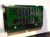
Program ROM mapping on PCB 0333-01-F1
01-front left edge pin 37
02-front left edge pin 38
03-front left edge pin 48 & level shifter (U13)
04-front left edge pin 49 & level shifter (U13)
05-front left edge pin 50 & level shifter (U13)
06-front left edge pin 51 & level shifter (U13)
07-front left edge pin 52 & level shifter (U10)
08-front left edge pin 55 & level shifter (U10)
09-front left edge pin 54 & level shifter (U10)
10-front left edge pin 53 & level shifter (U10)
11- +5V
12- +5V
13- PAL (U4 Pin 22)
14-back right edge pin 18 & resistor array (RP4) & level shifter (U8)
15-back right edge pin 10 & resistor array (RP4) & level shifter (U6)
16-back right edge pin 17 & resistor array (RP4) & level shifter (U8)
17-back right edge pin 05 & resistor array (RP4) & level shifter (U6)
18-back right edge pin 16 & resistor array (RP4) & level shifter (U8)
19-back right edge pin 06 & resistor array (RP4) & level shifter (U6)
20-back right edge pin 15 & resistor array (RP4) & level shifter (U8)
21-back right edge pin 07 & resistor array (RP4) & level shifter (U6)
----
22- GND
23-back right edge pin 14 & resistor array (RP6) & level shifter (U11)
24-back right edge pin 08 & resistor array (RP6) & level shifter (U9)
25-back right edge pin 13 & resistor array (RP6) & level shifter (U11)
26-back right edge pin 09 & resistor array (RP6) & level shifter (U9)
27-back right edge pin 12 & resistor array (RP6) & level shifter (U11)
28-back right edge pin 29 & resistor array (RP6) & level shifter (U9)
29-back right edge pin 11 & resistor array (RP6) & level shifter (U11)
30-back right edge pin 20 & resistor array (RP6) & level shifter (U9)
31- +5V
32- PAL (U4 Pin 21)
33-front left pin 39
34-front left edge pin 40 & level shifter (U15)
35-front left edge pin 41 & level shifter (U15)
36-back left edge pin 30 & front left edge pin 42 & level shifter (U15)
37-back left edge pin 27 & front left edge pin 43 & level shifter (U15)
38-back left edge pin 25 & front left edge pin 44 & level shifter (U14)
39-back left edge pin 24 & front left edge pin 45 & level shifter (U14)
40-back left edge pin 23 & front left edge pin 46 & level shifter (U14)
41-back left edge pin 22 & front left edge pin 47 & level shifter (U14)
42- PAL (U4 Pin 3)

nearly every Address and Data pin is routed to the edge connector in addition to a level shifter IC (most likely to be routed to the ASIC)
The exceptions are GVpp, A20, and A19, which are routed to the PAL and A18, A17, and A16 which are routed to the edge connector without a matching connection to the level shifter.

also interesting is that A8-A13 have 2 connections each on the edge connector.

the pal modifications seem to mostly bypass the PAL's control of of the last two address lines.
A20 is normally PAL controlled and we tie it high
A19 is normally PAL controlled and we tie it directly to the Edge connector
The only remaining connection between the program ROM and the PAL is Program ROM Pin 13 (GVpp)
 
Here is Espgaluda - Will get to Ketsui later tonight.
Thank you very much. This is the long awaited version using Killing blade with ARM chip removed. Seems that the only hacking made is two jump wires on the back on PRG pcb and custom PAL/program code??

Could you confirm the pcb number of GFX board? its blury in the first picture, but it seems different that one in my killing blade cart:

kiXOQIgl.jpg


This is #178
 
Last edited:
I think the graphics board may be custom made - my KB graphics board looks like yours.

Also, the jumper wire modifications aren't on the program ROM, they're on the PAL which has been removed. The ASIC is also gone suggesting that the main program ROM is ruining decrypted code

The other PAL looks like it might be original too
 
Last edited:
this is the EK-07.jed. It is actually hosted on JAMMArcade.net: http://www.jammarcade.net/files/pals/KOVSH_EK.U7.jed
and here is my dump of EK-08.jed

Code:
CUPL(WM)        5.0a  Serial# 60008009
Device          g16v8as  Library DLIB-h-40-2
Created         Wed Oct 24 06:37:53 2018
Name            ek_08
Partno          
Revision        
Date            
Designer        
Company         
Assembly        
Location        
*QP20 
*QF2194 
*G0 
*F0 
*L00000 11111011101110111011011111111111
*L00032 10110111101110111011011111111111
*L00256 01110111111110111011011111111111
*L00288 10110111101110110111011111111111
*L00320 10110111011111111011011111111111
*L00352 11111011101110110111011111111111
*L00384 11111111101101111011011111111111
*L00416 11111011011111111011011111111111
*L00448 01110111011101111011011111111111
*L01024 01111111111111111111111111111111
*L01280 10111011111111111111111111111111
*L01312 01110111111111111111111111111111
*L01536 01110111101111111111111111111111
*L01568 11111011011111111111111111111111
*L01600 10110111011111111111111111111111
*L01792 01110111111110111111111111111111
*L01824 11111011011110111111111111111111
*L01856 10110111011110111111111111111111
*L01888 11111011101101111111111111111111
*L01920 10110111101101111111111111111111
*L02112 00000000001100001111111111111111
*L02144 11111111111111111111111111111111
*L02176 111111111111111110
*C541A
*F58C
hope this helps. It is not a direct dump but was done using an adapter and reading it as an eprom. Then I ran it through an Optimizer and generated the .jed file. I did test it on an actual cart and it worked.
 
@EVAWINGZERO - Thank you very much for the photos :D

Any chance you have an EPROM programmer and are able to dump your main program ROM? (27C322 device)
 
Back
Top