Experimental PROGBK1 adaptation for 8MB on P2 CPU ROM

Joined
Jan 8, 2019
Messages
985
Reaction score
1,013
Location
Spain
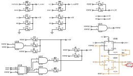
Hi. I have made a provisional schematic of how I think P2 rom latching works on Vortex cartridges with games higher than 1MB+4MB total CPU size, targeted to PROGBK1 original boards.

Esquemático Latch LS74.png


The idea is to add a new LS74 for latching D2 signal, which can improve P2 from 4MB to 8MB using the same logic as 64mbit C ROMs. (CE signal now is A21 new input bit). These following games are an example of big exceeding P2 4MB rom size:

Rage of the Dragons
Samurai Shodown V Special
SNK VS CAPCOM Chaos
The King of Fighters 2003

Theorically, catching the first 1MB of the joint PROM file of Vortex rom would be P1, and the rest of the info would be P2 (max 8MB). This is a test I want to do, but first I want to know if anyone knows if this type of latching is used in Vortex roms.

I have studied this possibility because I have seen in original roms that normally would use 1 x 27C160 PROM on P1 (2MB), the normal banking is catching the second MB as the main MB and the first MB as the banked MB. In Vortex roms this MBs are interchanged for following the logic of first MB - main MB, and the rest of the info as P2 ROM.

I don't think the new BANK2 signal has to be used on LS139 input logic for adapting P2OE signal, because by default P2OE signal is PORTOE (joint logic from PORTOEU and PORTOEL from LS08. ) It has nothing to do when referring to BANK0 and BANK1 signals, so BANK2 shouldn't be a problem to add.

Could it be possible to adapt bigger games to that logic/banking or are they adapted already?
 
Nice to see some one on work on this question :-D i'm really interested.
Thanks for that, keep us updated.
 
Also extremely interested - thank you for sharing this research.

I’m a NeoGeo learner, but if I understand correctly this is for “large” NeoGeo games where P1 = 4MB P2 = 4MB

So MS5 would be another example right?
 
Also extremely interested - thank you for sharing this research.

I’m a NeoGeo learner, but if I understand correctly this is for “large” NeoGeo games where P1 = 4MB P2 = 4MB

So MS5 would be another example right?
Metal Slug 5 is in Vortex as "Metal Slug 5 bootleg", which is a decrypted rom.

The games I use as an example have more than 4MB on P2 rom.
 
I'm having trouble with a much simpler implementation of this same idea.

Want to read 2MB SP2 on an AES PROG-TOP board
From the factory AES PROG-TOP will only read 1MB SP2

In theory this should be a simple matter of pulling D0, PORTWEL and RESET off the cart edge, merging them in a 74LS74, and outputting to SP2 A19 to switch between lower and upper
schematic1-png.60758.jpg

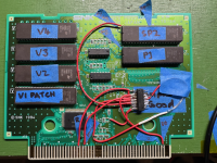
But... it doesn't work. Any ideas on what I'm doing wrong?
IMG_0951 (1).png
 
I archieved 1MB+4MB+4MB CPU on PROGBK1 boards half a year ago, for anyone to know. The last thing to do is to install level shifters for making a full correct roms protection.

PXL_20250413_105958972.jpg


@hatmoose About AES cartridges, I wouldn't know, because I haven't touched that format. Only MVS
And this project is accessible or shared in any location ?
Im interester in this kind of adapters.

Thanks
 
And this project is accessible or shared in any location ?
Im interester in this kind of adapters.

Thanks
For now they are for personal purposes, but when I complete the investigation I will take in mind if I free them. The first ones to use them are going the chinese, and I don't want them to access these so easily.
 
Good to know, I don't think the Chinese need technology like this, they use completely new cards.
Like this one:
1212.jpg

This is something for enthusiasts who want to do some homebrew or conversions.
 
I archieved 1MB+4MB+4MB CPU on PROGBK1 boards half a year ago, for anyone to know. The last thing to do is to install level shifters for making a full correct roms protection.
awesome work! I'd wanted to make such adapters for a while but never made it a priority.

any chance they allow programming through the adapter or do you have to remove chips to reprogram?
 
I see you're using MX29L3211MC-10 Flash EEPROMs. If you look at their datasheet, they specify that their operations are rated at 3.3V +/- 10% across Vcc, address and data. The Vortex carts use NOR Flash with max rating of Vcc + 2V! While you're using a 3.3V voltage regulator for all the flash, the data/address lines are still 5V.

The other trick Vortex has up its sleeve is that address lines all flow through the FPGA. The FPGA they use is a 5V rated part. I believe it's being used as a voltage translator to the flash (for the address lines at least)

Given you made your own daughter board with new flash, have you considered adding voltage translators? or has the cart been stable enough?
 
awesome work! I'd wanted to make such adapters for a while but never made it a priority.

any chance they allow programming through the adapter or do you have to remove chips to reprogram?
I flash the roms before soldering.

I see you're using MX29L3211MC-10 Flash EEPROMs. If you look at their datasheet, they specify that their operations are rated at 3.3V +/- 10% across Vcc, address and data. The Vortex carts use NOR Flash with max rating of Vcc + 2V! While you're using a 3.3V voltage regulator for all the flash, the data/address lines are still 5V.

The other trick Vortex has up its sleeve is that address lines all flow through the FPGA. The FPGA they use is a 5V rated part. I believe it's being used as a voltage translator to the flash (for the address lines at least)

Given you made your own daughter board with new flash, have you considered adding voltage translators? or has the cart been stable enough?
Yeah, my intention is to implement level shifters for all data input and output for the roms
 
Its also interesting to play with your C/V adapter for SOP44 rom.
Can be shared ?
Maybe its need also level shifters for in/out
 
Last edited:
Back
Top