

So as promised I have finished the pinout of a CPS3 32/128Mb SIMM PCB. Again, for reference I took a photo of the SIMM and numbered the flash ICs accordingly since there is no "official" numbering on the silkscreen of the PCB.
Anyway, the 128 Mbit SIMM has 8 x 16Mbit Fujitsu flash ICs. 4 x Normal pinout and 4 x Reverse pinout. The normal pinout ICs are of type MBM29F016-90PFTN and the reverse pinout ICs are of type MBM29F016-90PFTR
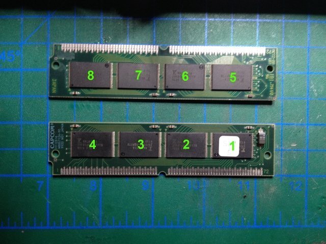
Front:
IC1: Reverse pinout
IC2: Normal pinout
IC3: Reverse pinout
IC4: Normal pinout
Back:
IC5: Normal pinout
IC6: Reverse pinout
IC7: Normal pinout
IC8: Reverse pinout
The 32 Mbit SIMMs I have only IC1 and IC6 populated. Yes, I know the 32Mbit SIMM picture on the CPS3 - Wiki on the "Arcade Otaku Wiki" is somehow different. It might be from early CPS3 production or from late CPS2 (all-in-one black boards) production.
Here is the pinout of the 32/128Mbit SIMM PCB;
As you can see it is totally different than the 64Mbit SIMM module. This PCB controls the flash ICs in pairs (4 total /CE signals controlling 8 x flash ICs in pairs) and there are two sets of data bus where on a 64Mbit SIMM all the flash ICs have their data pins connected seperately and there were only one common /CE signal...
Anyway, the 128 Mbit SIMM has 8 x 16Mbit Fujitsu flash ICs. 4 x Normal pinout and 4 x Reverse pinout. The normal pinout ICs are of type MBM29F016-90PFTN and the reverse pinout ICs are of type MBM29F016-90PFTR
Front:
IC1: Reverse pinout
IC2: Normal pinout
IC3: Reverse pinout
IC4: Normal pinout
Back:
IC5: Normal pinout
IC6: Reverse pinout
IC7: Normal pinout
IC8: Reverse pinout
The 32 Mbit SIMMs I have only IC1 and IC6 populated. Yes, I know the 32Mbit SIMM picture on the CPS3 - Wiki on the "Arcade Otaku Wiki" is somehow different. It might be from early CPS3 production or from late CPS2 (all-in-one black boards) production.
Here is the pinout of the 32/128Mbit SIMM PCB;
| Pin | Conn. | Note |
| 1 | Vcc | Common |
| 2 | Vcc | Common |
| 3 | D7 | IC1, IC2, IC3, IC4 |
| 4 | N.C. | |
| 5 | D6 | IC1, IC2, IC3, IC4 |
| 6 | N.C. | |
| 7 | D5 | IC1, IC2, IC3, IC4 |
| 8 | N.C. | |
| 9 | D4 | IC1, IC2, IC3, IC4 |
| 10 | N.C. | |
| 11 | GND | Common |
| 12 | D3 | IC1, IC2, IC3, IC4 |
| 13 | N.C. | |
| 14 | D2 | IC1, IC2, IC3, IC4 |
| 15 | N.C. | |
| 16 | D1 | IC1, IC2, IC3, IC4 |
| 17 | N.C. | |
| 18 | D0 | IC1, IC2, IC3, IC4 |
| 19 | N.C. | |
| 20 | GND | Common |
| 21 | D7 | IC5, IC6, IC7, IC8 |
| 22 | N.C. | |
| 23 | D6 | IC5, IC6, IC7, IC8 |
| 24 | N.C. | |
| 25 | D5 | IC5, IC6, IC7, IC8 |
| 26 | N.C. | |
| 27 | D4 | IC5, IC6, IC7, IC8 |
| 28 | N.C. | |
| 29 | GND | Common |
| 30 | D3 | IC5, IC6, IC7, IC8 |
| 31 | N.C. | |
| 32 | D2 | IC5, IC6, IC7, IC8 |
| 33 | N.C. | |
| 34 | D1 | IC5, IC6, IC7, IC8 |
| 35 | N.C. | |
| 36 | D0 | IC5, IC6, IC7, IC8 |
| 37 | N.C. | |
| 38 | N.C. | |
| 39 | A20 | Common |
| 40 | A19 | Common |
| 41 | A18 | Common |
| 42 | A17 | Common |
| 43 | A16 | Common |
| 44 | A15 | Common |
| 45 | A14 | Common |
| 46 | A13 | Common |
| 47 | A12 | Common |
| 48 | A11 | Common |
| 49 | GND | Common |
| 50 | A10 | Common |
| 51 | A9 | Common |
| 52 | A8 | Common |
| 53 | A7 | Common |
| 54 | A6 | Common |
| 55 | A5 | Common |
| 56 | A4 | Common |
| 57 | A3 | Common |
| 58 | A2 | Common |
| 59 | A1 | Common |
| 60 | A0 | Common |
| 61 | GND | Common |
| 62 | /RESET | Common |
| 63 | GND | Common |
| 64 | /CE | IC4, IC7 |
| 65 | /CE | IC3, IC8 |
| 66 | /CE | IC2, IC5 |
| 67 | /CE | IC1, IC6 |
| 68 | GND | Common |
| 69 | /WE | Common |
| 70 | N.C. | |
| 71 | /OE | Common |
| 72 | N.C. |
As you can see it is totally different than the 64Mbit SIMM module. This PCB controls the flash ICs in pairs (4 total /CE signals controlling 8 x flash ICs in pairs) and there are two sets of data bus where on a 64Mbit SIMM all the flash ICs have their data pins connected seperately and there were only one common /CE signal...
Last edited:


