DCrosby
Enthusiast
So to try and both help others and try and solve my own issue, I wanted to A: Make sure I have my info correct B: Try and help others no matter what the code is, and share my understanding thus far.
So: First things first...
The Address Matters, as if it's failing right off the bat Address 00000000 then it's something with the lines/wires, or the chips are bad, as it can't even begin to write, if it's something later on, as each address is another page of memory... so something (anything) other than 000000 like 0004533451 or something will indicate it got that far into the ram before something bad happened.
Ok... so a 5555 would look something like this in Binary:
0101 0101 0101 0101
you can use a hex to binary converter to get that number....
5540 looks like this:
0101 0101 0100 0000
so if we put them on top of each-other we can see a pattern...
These values with the ^ are divergent / wrong from what we expect... so what does that mean?
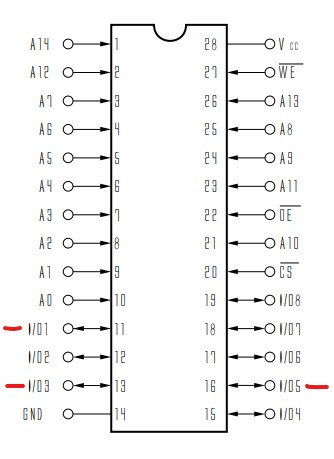
This is the pin-out of the memory chip, each chip has 8 data lanes, I/01 - I/08 and 2 chips = 16 bits.
The error FFFF written FF40 tells us the lower ram is affected.
if the error would have been FFFF written 40FF read it'd be the Upper Ram at fault.
So lets look at one of the ram chips (Both Upper and lower are identical in pin assignment but not what they're connected to):

I believe (reading from the back of the binary sequence) the last number being pin 1, then pin2 pin 3 etc...
So reading this lines 1,3,& 5 are not communicating properly. we can now trace where those go, and if the connection is solid.
There are other lines that can affect the chip, which then run through the HC32, which then toggles WE = Write Enable, CS = Cable Select (from the Pro-CO chip pins 8 and 16 depending which chip high or low is being selected) so other things can affect the chips function, but from the standpoint of what is the error it's telling you a bunch of which chip, and which lines. It's important to check that those lines are good, and are not damaged or pinched, as higher resistance, or intermittent connections can cause these kinds of issues.
So on to my issue, I've checked everything as far as I can, I've replaced the HC32, Both Surface Mount Backup Ram's (The two memory chips in the row 9 closest to the jamma edge. And I've not been able to clear the error, I may try tomorrow to turn on all dips to see if I can clear the backup ram, but it's pretty frustrating when you've checked and double checked things, and have no idea what's causing the error...
I'm also seeing either activity or static values on all the ram pins. I may go back tomorrow and make sure that none of the address lines in or out, are static, and it's only certain pins like GND that are static low etc...
So: First things first...
The Address Matters, as if it's failing right off the bat Address 00000000 then it's something with the lines/wires, or the chips are bad, as it can't even begin to write, if it's something later on, as each address is another page of memory... so something (anything) other than 000000 like 0004533451 or something will indicate it got that far into the ram before something bad happened.
Ok... so a 5555 would look something like this in Binary:
0101 0101 0101 0101
you can use a hex to binary converter to get that number....
5540 looks like this:
0101 0101 0100 0000
so if we put them on top of each-other we can see a pattern...
| 0101 | 0101 | 0101 | 0101 |
| 0101 | 0101 | 0100 | 0000 |
| ---- | ---- | ---^ | - |
This is the pin-out of the memory chip, each chip has 8 data lanes, I/01 - I/08 and 2 chips = 16 bits.
The error FFFF written FF40 tells us the lower ram is affected.
if the error would have been FFFF written 40FF read it'd be the Upper Ram at fault.
So lets look at one of the ram chips (Both Upper and lower are identical in pin assignment but not what they're connected to):
I believe (reading from the back of the binary sequence) the last number being pin 1, then pin2 pin 3 etc...
So reading this lines 1,3,& 5 are not communicating properly. we can now trace where those go, and if the connection is solid.
There are other lines that can affect the chip, which then run through the HC32, which then toggles WE = Write Enable, CS = Cable Select (from the Pro-CO chip pins 8 and 16 depending which chip high or low is being selected) so other things can affect the chips function, but from the standpoint of what is the error it's telling you a bunch of which chip, and which lines. It's important to check that those lines are good, and are not damaged or pinched, as higher resistance, or intermittent connections can cause these kinds of issues.
So on to my issue, I've checked everything as far as I can, I've replaced the HC32, Both Surface Mount Backup Ram's (The two memory chips in the row 9 closest to the jamma edge. And I've not been able to clear the error, I may try tomorrow to turn on all dips to see if I can clear the backup ram, but it's pretty frustrating when you've checked and double checked things, and have no idea what's causing the error...
I'm also seeing either activity or static values on all the ram pins. I may go back tomorrow and make sure that none of the address lines in or out, are static, and it's only certain pins like GND that are static low etc...
Last edited:
