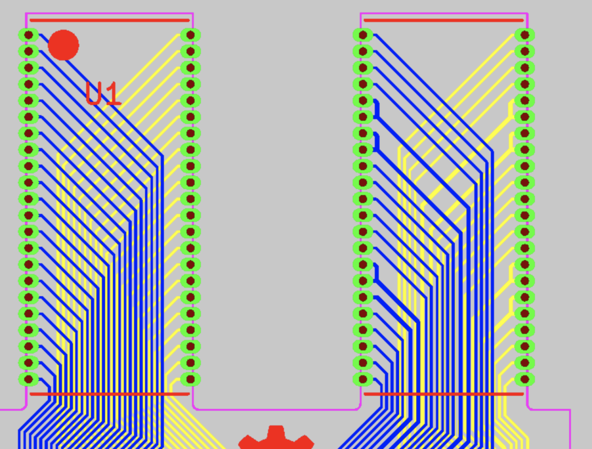
I too have the FR-300 so 0.6mm is not an option. But I have a professional hot air station. After you apply some fresh solder (it seems the factory uses lead free) set the station at 450C and go at it. Keep it moving (the space between the pins can bubble up, but will shrink back down as it cools, which is no big deal as it's a 2 layer PCB). I was able to remove the daughter board with no issues.
You are using an out of date browser. It may not display this or other websites correctly.
You should upgrade or use an alternative browser.
You should upgrade or use an alternative browser.
- Thread starter goguelnikov
- Start date
xodaraP
Legendary
I too have the FR-300 so 0.6mm is not an option. But I have a professional hot air station. After you apply some fresh solder (it seems the factory uses lead free) set the station at 450C and go at it. Keep it moving (the space between the pins can bubble up, but will shrink back down as it cools, which is no big deal as it's a 2 layer PCB). I was able to remove the daughter board with no issues.
I tried this and got a fair way with the hot air alone. I got to having them about half way removed and then the power and ground pins just wouldn’t budge further
I ended up with a big burnt patch on the solder mask trying to get them to move further
I tried this and got a fair way with the hot air alone. I got to having them about half way removed and then the power and ground pins just wouldn’t budge further
I ended up with a big burnt patch on the solder mask trying to get them to move further
This happened to me with the first one. For the next 2, here's what I did:
- added fresh 60/40 solder to all the pins, use lots of flux (use higher temp than you normally use. You want to mix the lead solder with the lead free)
- bring hot air station to 480C and about medium speed
- prop the board in the air. Have a too that can fit between the adapter and PCB on the other side
- start heating the 2 rows of pins - IMPORTANT: Do not get hot air between the 2 rows. You will burn the PCB
- continue for about 60s, and then start pushing the tool
- after 2 minutes the adapter will fall off.
Add fresh solder to all the holes, and use your FR300 or other desolder tool to suck the solder out (cleaning the holes). I also ran braid against the pins just to remove and solder that stuck to the pins of the adapter. You should be able to push the adapter back as a test. To remove, always push the pins out before trying to pull it out.
This technique I find to be very fast and ends up in very clean PCB and clean holes.
Good luck.
XML:
    <software name="menu">
        <description>Menu</description>
        <year>2023</year>
        <publisher>ArcadeTV</publisher>
        <info name="serial" value="NGM-161 (MVS)"/>
        <info name="release" value="20231011 (MVS)"/>
        <info name="alt_title" value="Menu"/>
        <sharedfeat name="release" value="MVS" />
        <sharedfeat name="compatibility" value="MVS" />
        <part name="cart" interface="neo_cart">
            <dataarea name="maincpu" width="16" endianness="big" size="0x100000">
                <rom loadflag="load16_word_swap" name="menu-p1.bin" offset="0x000000" size="0x100000" crc="1a759428" sha1="f4ff6fc33475afb8e40409febb4dbcda56cb25a4" />   <!-- MB834200 -->
            </dataarea>
            <dataarea name="fixed" size="0x040000">
                <rom offset="0x000000" size="0x020000" name="menu-s1.bin" crc="c2ea0cfd" sha1="fd4a618cdcdbf849374f0a50dd8efe9dbab706c3" />   <!-- TC531000 -->
            </dataarea>
            <dataarea name="audiocpu" size="0x010000">
                <rom offset="0x000000" size="0x010000" name="menu-m1.bin" crc="25058131" sha1="705241b9c1a6b1d3b031e863910bd70263637857" />   <!-- MB832000 -->
            </dataarea>
            <dataarea name="sprites" size="0x200000" />
        </part>
    </software>
Here's a Beta version of the alternative MENU as a proof of concept.
Thanks to @Vortex for all his efforts!
Instructions:
- add the XML to your MAME\hash\neogeo.xml
- copy and optionally extract the attached file to MAME\roms (results in MAME\roms\menu\*.bin)
- start mame via commandline: mame.exe neogeo -cart1 menu
FYI, if you have your bios set to JAP region there will be issues. The rom will show different game titles depending on the system's region - I was just too lazy preparing both lists at this moment.
The gamelist is dynamic and is included from an external file which is subject to being generated by either the compiler or a script/tool/batch, whatever works.
I'll post the source on github in the next step.
Attachments
Last edited:
@ack when dumping the original CROM and getting the E: number going up, this means that there's something wrong? Maybe a broken trace of the stock interposer to the chip?
I dumped one of the CROM's from the CHR board, and got E=0 at the end. I did an md5 test on it and I got this:
20827f2a24a4b6825baa4ad030eb2f26 crom.bin
I got the same md5 both under Windows 7 MD5 utility as well the the md5 utility build into OSX. Wonder why it's different than yours.
I dumped one of the CROM's from the CHR board, and got E=0 at the end. I did an md5 test on it and I got this:
20827f2a24a4b6825baa4ad030eb2f26 crom.bin
I got the same md5 both under Windows 7 MD5 utility as well the the md5 utility build into OSX. Wonder why it's different than yours.
Last edited:
I've added a method for generating custom gamelists in the menu for the time as long as it is not linked with the compiler output.
Please see the readme on github for details.
https://ngmenu.arcade-tv.de/
Please see the readme on github for details.
https://ngmenu.arcade-tv.de/
The dumper firmware will read each address twice and if the data doesn't match it will increment the error count "E". If it doesn't match the firmware will also go into a loop reading the address over and over until 2 consecutive reads read the same data.@ack when dumping the original CROM and getting the E: number going up, this means that there's something wrong? Maybe a broken trace of the stock interposer to the chip?
I dumped one of the CROM's from the CHR board, and got E=0 at the end. I did an md5 test on it and I got this:
20827f2a24a4b6825baa4ad030eb2f26 crom.bin
I got the same md5 both under Windows 7 MD5 utility as well the the md5 utility build into OSX. Wonder why it's different than yours.
I'm not sure on the md5. Those are the values I got.
Those M1/S1 flash chips where the most troublesome for me. Its very easy to break off a leg on them.I took E=0 to mean there were no errors during dumping. My S1 chip came up with E=298354 or something so it was toast
Those M1/S1 flash chips where the most troublesome for me. Its very easy to break off a leg on them.
I actually found the M1/S1 to be super easy (I have a Quick style professional hot air station) I also verified the MD5 dumps from them match with what you posted. Biggest challenge was figuring out orientation (as pin 1 is not marked on the IC) But I matched the text orientation on IC and dumper and that worked.
I'm waiting for your replacement daughterboards to come in; at this point, I don't plan on using the one that came with the cart, the surface mount legs are just too fragile for the number of insertions that need to happen. Their biggest flaw is that it's impossible to get all the solder off the pins, so the legs get stuck in the sockets (e.g. dumper PCB) resulting in them being ripped out.
I was successful in dumping/programming using your dual daugherboard CROM-1. Thank you for sharing the PCB designs!!
@ack have you noticed that some of the ICs (in particular PROM) are of questionable quality. I got a couple that have 1-2 errors on dump, or verify, but when I try again, it passes 100%.
For example, I dumped PROM-1, and it had 1 E. So I decided to do an MD5 check on it, and it has the exact checksum as your dump! So not sure if I should ignore 1 error or what.
For example, I dumped PROM-1, and it had 1 E. So I decided to do an MD5 check on it, and it has the exact checksum as your dump! So not sure if I should ignore 1 error or what.
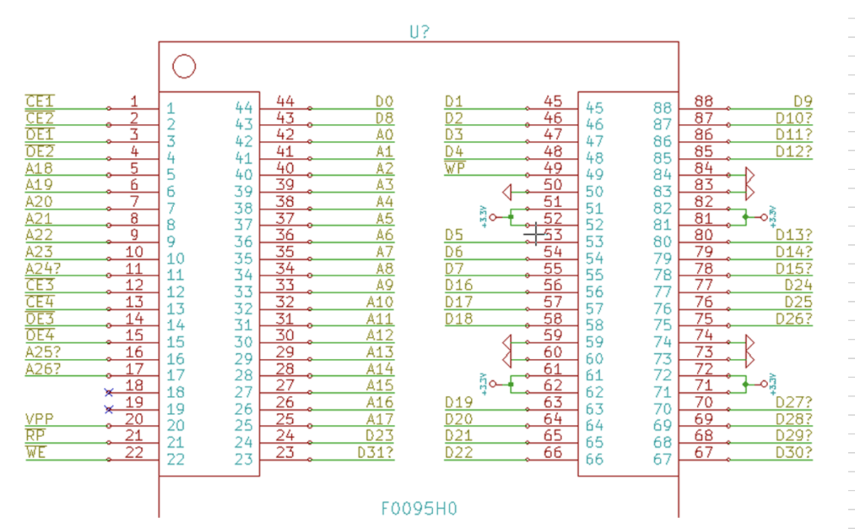
I'm comparing the schematics @Vortex provided in his spreadsheet and comparing it to the schematics that @ack created for the daughterboard. If I'm not mistaken, pin 1 on the excel spreadsheet is in the wrong spot. It marked at the top left, but I believe it has to be in the bottom left. Take a look at the 2 right columns, especially where the 2 pins next to one another are connected. It only makes sense if the pin 1 is where I believe it should be. Thoughts?


Not everyone has unibios.
I wonder how it's done in MultiMVS/AES and NeoSD... (I don’t think that they patch the proms on the fly during flashing ...)
The NeoSD has an in-game-reset to menu: player 1 A + D + Start
So at this time, to get back to the main menu one has to do a full power cycle?
That confused me we well. It seems like the original image of the symbol thats been floating around has pin 1 marked in the wrong location. Its almost like the person that made it flipped the chip so the pads were facing up when making the symbol but for got to realize that would mean pin 1 would also change from being at the top left to the bottom left. Since I had to remake the symbol for it in kicad for my daughterboard projects, I just corrected the issue.I'm comparing the schematics @Vortex provided in his spreadsheet and comparing it to the schematics that @ack created for the daughterboard. If I'm not mistaken, pin 1 on the excel spreadsheet is in the wrong spot. It marked at the top left, but I believe it has to be in the bottom left. Take a look at the 2 right columns, especially where the 2 pins next to one another are connected. It only makes sense if the pin 1 is where I believe it should be. Thoughts?
AES cart has shown up and seems to be working. Let me know where/what you need measured @ack and I'll get it done today.AES cart should arrive this week for measurements @ack , but my MVS ones showed up yesterday.
I think just taking a picture of the front/back of each of the boards should be good.AES cart has shown up and seems to be working. Let me know where/what you need measured @ack and I'll get it done today.
thanks

