What's new
Hi Alex,

Thanks for your reply.

To proceed with castellated holes processing, you will need to modify your Gerber files to meet the requirements shown in the below image, and there will be around 35USD extra cost per order. Shall we activate replace file button for you to modify your files and send you extra cost to pay?

Or should we proceed with normal process with the risk of possible defects? Please kindly advise.

eb9-8b43-1c23-3a000001dc00&sig=lGZFGn69ZbttKzg9RA6.jpg

mail?url=https%3A%2F%2Fwww.jlcpcb.jpg


Best regards
Olivia

i know @ManCloud received same answer about manufacturing , but maybe this can help for the future .

I proceed on JLCPCB to normal process (like how the zip is on github)

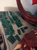
This is for guys who wants castellated 0.8mm thickness for 161 in 1 daughter boards to be manufactured, with 35$ usd additional cost - 5 x double daughter boards =>

so the price can be 42 : 5 = 8.4$ USD
 
You just need to proceed with known defects, Vortex mentioned this earlier - then you need to push the castellated holes into the grooves on the PCB to prevent bridging
 
I have managed to get my S1 chip reconnected with a bridge wire and this is now programmed so I am all ready to go except for the C ROMs

For anyone that has done so, what is the best way to attach the C ROM chips to the daughterboards? I've got them removed from the original daughterboards but I can't get them onto the new daughterboards with reliable connections

The pads on the edges fall off at the lightest touch from the soldering iron, should I be loading solder onto the pads on the chip itself and using hot air to attach to the daughterboard?
 
The pads on the edges fall off at the lightest touch from the soldering iron, should I be loading solder onto the pads on the chip itself and using hot air to attach to the daughterboard?
Are you running your iron really hot? I'm running about 275C when doing these. I'm also using a VERY small tip (0.1mm).

then you need to push the castellated holes into the grooves on the PCB to prevent bridging
This caused more trouble for me than not doing it. It was easier to /only/ push the ones in that were already broken. Then gob flux paste onto it.

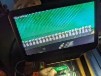
Heat the pad on the PCB, get a small blob of solder on there, move the iron to the side of the castellated copper bit and heat that until all the flux bubbles out of the solder, then feed more solder into the hole. It'll get sucked down into the pad of the chip. If it's really stubborn I'll heat the pin directly after doing the above.

Video explanation:
https://photos.app.goo.gl/2KtMEFJJt3gzCQjb7

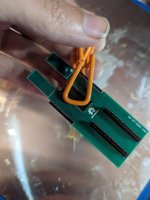
I'm also using a chip bag clip to hold the chip in place while I lay down the first side.

PXL_20231118_044237529.jpgPXL_20231118_044226933.jpgPXL_20231118_044706843.jpg
 
Last edited:
I was running a higher temperature since the holes are so small, but I have reduced this down now due to losing all of the pads on my attempts

What you are doing is exactly what I am doing, but some pads just WILL NOT read a connection even when it looks like a solder bridge is present, I'm at a complete loss for how to proceed here. I don't have a microscope which I don't think is helping. I think I'm beyond the limits of soldering by eye here

The sides with the castellated holes are not an issue even after pushing these in, it's the sides with just the small pad on the edge present - it's possible the way the PCBs have been made there is just not enough copper for a proper connection present
 
I don't have a microscope which I don't think is helping. I think I'm beyond the limits of soldering by eye here
It certainly wouldn't be accomplishable without one for me. And it's harder to check what's going wrong when you can't see it happening in the moment and have to keep going back to using a phone to take a zoomed in picture.

The sides with the castellated holes are not an issue even after pushing these in, it's the sides with just the small pad on the edge present - it's possible the way the PCBs have been made there is just not enough copper for a proper connection present
Interesting we had completely opposite issues. I'm not really sure how to advise beyond what I had. I did try starting on the pads of the chip, and going up to the castellated sides and letting it suck up in there, but that lead to way more bridging between pads so I abandoned that approach pretty quickly.
 
Yes I found that problem, I've been trying to use drag soldering with a big blob on a larger tip and loads of flux, but it's not filling the castellated holes and I don't seem to be getting a good connection at all. Zooming in on photos I appear to have a connection, but when checking with a multimeter I'm reading several NC pins and when connected to the programmer I just get

E: 4
CRC: 0000000010

There are pads on the underside of the PCB and I was hoping that I would get a connection on that side, but I'm definitely not. Power and ground pins as always seem to be the biggest issues

Any chance you would sell me a completed set of C ROM chips? I can send you the ones I have for use on another board, but I just don't think I'm going to be able to accomplish this
 
I think I can explain why we are having opposite issues. I just pulled out one of the dual daughterboards and all 4 sides have the castellated holes. On the single chip repro daughterboards 2 sides have these and 2 sides have very tiny pads

I might try a dual daughterboard and see if I get a different result

Edit: Dual daughterboard worked first try. I've literally been fighting with these all day :(

Further edit: Trying to dump or prog now and it's throwing a huge number of errors immediately so something isn't happy. The checksum is coming back correct though

Further edit: I built another daughterboard, adapter board and used a different chip and I am getting solid connections on these dual IC PCBs - damn I wasted way too much time and too many headers trying to get the single ones to work :(
 
Last edited:
Further edit: I built another daughterboard, adapter board and used a different chip and I am getting solid connections on these dual IC PCBs - damn I wasted way too much time and too many headers trying to get the single ones to work :(

The single daughterboard is easy to work with, once you figured out the technique. Look at it under a microscope and use the tip of an exacto knife to clear the cut holes. In some cases it's just getting the fibreglass filler out, in some cases you need to cut out the extra copper ring left behind. You need to check both sides of the PCB for any left over copper. Finally, flip the PCB on its side and check all 4 edges. You should see clear copper in the holes (no fibreglass) and no 2 holes are touching (just clean fibreglass wall between the holes)

I find working with the dual daughterboards to be more time consuming; especially when you try to align the 2nd flash chip.

getting the ICs mounted and unmounted is actually the easy part. Wait till you start programming them and realize the China cr4p connectors are not really rated for multiple insertions; especially on the programmer. You'll get a ton of errors and at some point need to replace the ports on the programmer .. after doing only a handful of flash chips. :(
 
@Vortex
May I ask if or what was edited in the AES menu?
Since there is no BackupRAM in the machine I guess it's just the replacement of the MCU routines, right?

Thank You very much!
@Vortex may I please ask that question again?
Can you tell what was edited in the AES menu, compared to the MVS menu?
Thank You!
 
Last edited:
I''m glad you're up and running @xodaraP !!!!

Not quite, still getting errors when trying to dump or program. But getting closer at least

The single daughterboards I made didn’t have holes on all 4 sides

Not sure if there was a manufacturing issue or if the design I used has been improved but having checked these against the dual boards these were never going to work
 
Not sure if there was a manufacturing issue or if the design I used has been improved but having checked these against the dual boards these were never going to work
I'm using Ack's, and they look the same as the dual ones but without the extra chip space. I haven't made many though, as I'm not having any real struggles with the STILT daughterboards.

I can send you some if you'd like. I ordered 150, but so far have used 3 because the STILTs seem just fine if you remove them with care.
 
I also used ack’s so likely a manufacturing issue

All good, the dual ones are working fine and I can cut them down to make single boards

I’ve ordered a whole new cart to do this properly. I’m just going through the process on the one I ruined so I don’t make the mistakes on the new one, or if I do, knowing how to fix it
 
Just dumping one now to try it - but I think I've got it

After I soldered the headers onto the daughterboard, I have hit them with hot air to make sure the solder has flowed to all through holes fully - this time on the board I previously got an error checksum, I have the correct checksum and at 15% no errors dumping so far. I will program this chip then move onto the next one and do the same there, then just need to make up one more for the V ROM chip

Definitely good practice for the real deal when the new cart arrives and if I can get this one running with a more limited game library in the meantime I can play some games until it arrives

Edit: Dump successful, now programming. This is going to take a while
 
Last edited:
After I soldered the headers onto the daughterboard, I have hit them with hot air to make sure the solder has flowed to all through holes fully - this time on the board I previously got an error checksum, I have the correct checksum and at 15% no errors dumping so far. I will program this chip then move onto the next one and do the same there, then just need to make up one more for the V ROM chip

The programmer is very iffy. I believe the checksum just does a quick sanity checks. As long as the required pins are connected, you'll get a good response; but it doesn't mean all the pins are connected. I've also seen cases where "verify" gives errors. I then do a "dump" and an md5sum check on the dump and it's identical to the original ROMs.

I've also had cases where the checksum failed, but chip worked great. I suspect this is due to all these components being pulls from old arcade PCBs and not new components.

Indeed. I am not worried if it says 1 error, but when I attempt a dump and the error count immediately goes up into the millions - something is not connected

I got the V ROM mounted onto a board now and it had E:1 on the Test V-ROM page but I'm dumping it now and 0 errors so far. Checksum was correct on the test page so I think we're good for this one. 1 more C ROM left that is on a board now but I will need to remove and attach to a new board
 
The programmer is very iffy.
I've run verify and had it give 0 errors, then a second time it gives infinite errors. Checking md5 after dumping seems to be the only real way to verify. :/
 
I've just programmed the V-ROM and the verify is giving infinite errors. Time to dump and check MD5 I guess
 
Back
Top