What's new

HardAzRockz

Enthusiast
Joined
Jul 25, 2020
Messages
183
Reaction score
135
Location
Tucson, az
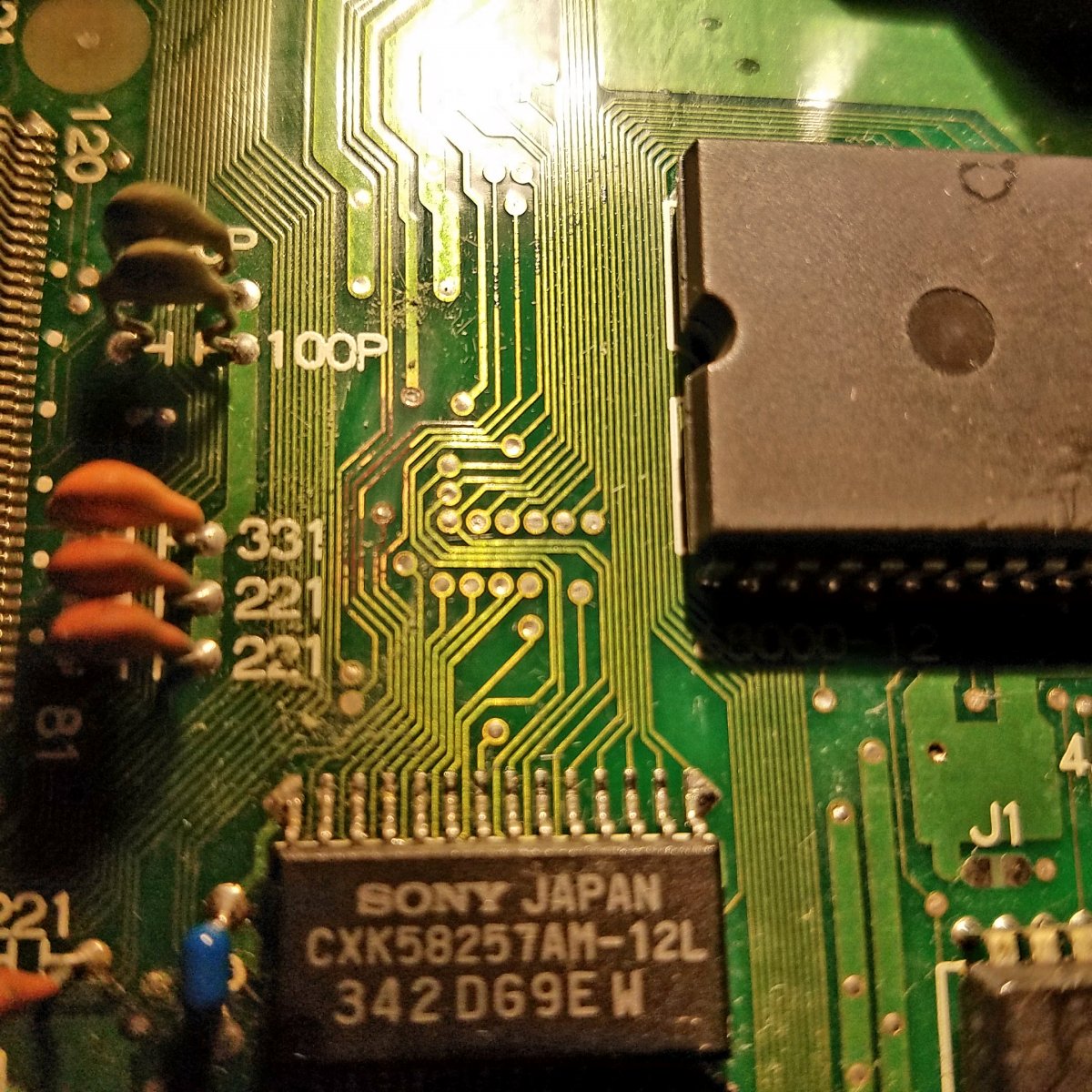
I recently purchased this faulty AES and determined to repair it. I've looked over the board and only found one area with corroded traces. I haven't had much time to do a continuity test yet. The BIOS are original and haven't been removed. I havent seen any damaged traces beside the ones pictured below. The board looks untouched for the most part. Can anyone give me an idea where to look beside these traces. Thanks
Screenshot_20210507-142646.png
20210507_132147.jpg
 
I replaced the bios with Unibios 4.0. No damaged traces100% in the bios area. I went around around the Neo B1 and LSPC2 A2 with my iron and reflowed the pins( no bridges). I cleaned the slot multiple times with contact cleaner. I clean the dirt around the board. I'm not seeing any damaged traces except the corroded traces in the above pic. I hit them with a fiberglass pen and applied some solder. They all seem to have continuity. I'm not sure what else to try. Can someone please help? here is a link to my video displaying the graphical glitches.
View: https://www.youtube.com/watch?v=LBeGinj_Dkg
 
Well I made some progress. I used B1 a fiberglass pen around the pads where the trace and pin connect. I also reworked some of the traces that had corrosion before. I'm getting close but still needs work. Have a look
View: https://youtu.be/rX8EsiHo5bQ
20210509_044023 (1).jpg


There is some flicker in the text below. I'm not entirely sure its not the game. I only have that game until Dark makes more AES Multis. Anyone?
 
Last edited:
The fact that the error is present not only on the BIOS but also on the game, means to me that the problem is somewhere else in the video section. If the RAM test passed well, then go for some of the chips in the video area.
 
Neo Geo does not use the RAM to draw the graphics, the graphics are read from the C and S1 ROMs.

The video ram is tables which tell the graphics chip where on the graphics ROMs it has to read the data.

So your target is the connections between the cartridge slot and the graphics chips (A and B chips)

The 2nd generation Neo Geo chipset (Fujitsu) is divided in three chips: (very simplified description)

A chip is the LSPC, performs control of the graphics hardware, generates video timings and interfaces with the video ram, since it controls the video ram it also defines where the graphics are read. Since the correct patterns are displayed on the screen (blocks are correct in placement at the screen) this part seem to be ok.

B chip is the actual video generator, it handles paletes and pixels. It also does the watchdog stuff. Since this one processes the pixels it receives the data from the C and S1 roms. Have this one checked for severed traces.

C chip is the 68000 bus control, controller ports control and the sound interface management chip. This part is fine right now apparently.
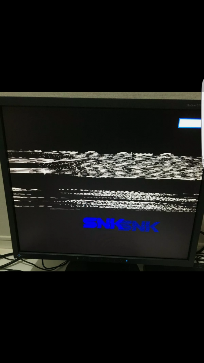
 
I've combed over this board several times I'm not seeing severed or damaged traces. The traces I repaired all have continuity. The B1 had some corrosion on the corner. I went over it with a fiberglass pen then reflowed the pins. I'm not seeing any other possible traces. Maybe those capacitors near the B1 are bad? Any clues what to look for beside bad traces? Is there traces under the B1? Maybe I should remove that?
 
If you have some microscope check the B1 pins/trace or directly reflow them using great smd flux. Sometimes the trace repair do not permit the signal to pass correctly. Also check if traces do not have contacts each others. Try using thin patch cable to be sure.
 
Hi,

Reflow neo-b1 chip using great flux ?
https://wiki.neogeodev.org/index.php?title=NEO-B1

Graphic issue on aes 3-6 root cause B1
https://www.neogeo-system.com/t3792-tuto-graphic-glitches
Yes I Reflowed the B1. It had corrosion on the corner. I check the pins are making contact with pads and no bridged. I think it's the trace near the B1 I repaired. I sanded them down with a fiberglass pan and then I ran some solder over the traces that looked bad I used strand of wire from a wire
 
It's not the B1 I checked it with my microscope several times. Maybe you're right about the traces
 
trace repair could be sometimes great but you cannot be sure contact is great. for sure in upper picture, traces are not great for me (what
also try to clean pcb between trace to avoid contact issues.

What is the root cause of this trace corrosion ?

try to avoid signal issue using direct end to end patch cables for each suspect lines. That what I will do first. (9x lines to confirm).

then, when issue will be confirmed, you will know what to do.

Is my trace repair just shit?
20210510_124954.jpg
20210510_125002.jpg
 
trace repair could be sometimes great but you cannot be sure contact is great. for sure in upper picture, traces are not great for me.
also try to clean pcb between trace to avoid contact issues.
try to avoid signal issue using direct end to end patch cables for each suspect lines. That what I will do first. (9x lines to confirm)
I think you're right. Im gonna jump some 30ga kynar wires. I'll report back
 
Back
Top