This post describes using various tools from https://github.com/buffis/cv1k_research to fix CV1000 pcbs with bad NAND flash for U2.
- Background
A while ago there was a Espgaluda 2 sold on YAJ that had sprite issues when bombing. https://page.auctions.yahoo.co.jp/jp/auction/x1005199728
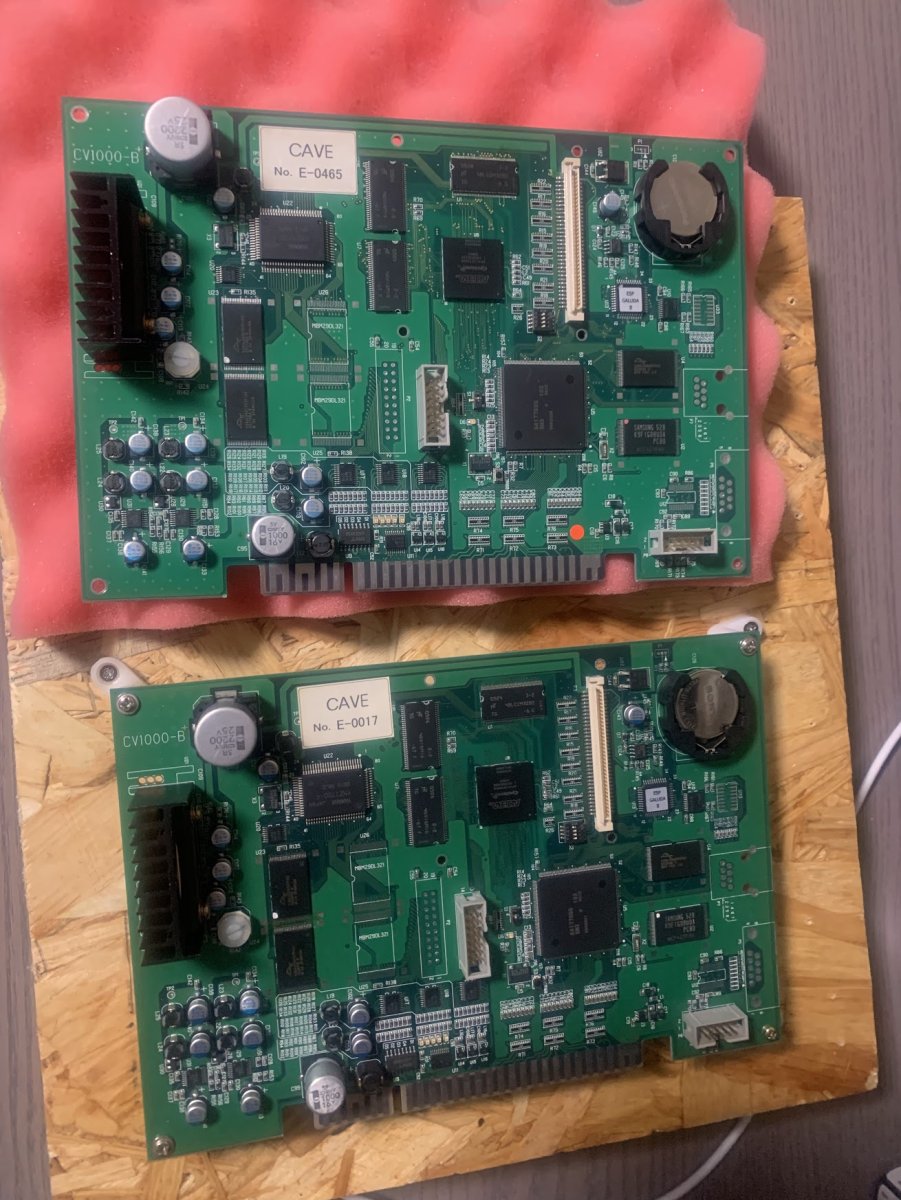
I was looking at it, but price was a bit too high to me to justify getting it since I already have galuda2 on pcb, but the dude that ended up buying it agreed to send it to me to have a look at it, since I had a exciting idea for how to fix it using JTAG, without having to do any soldering!
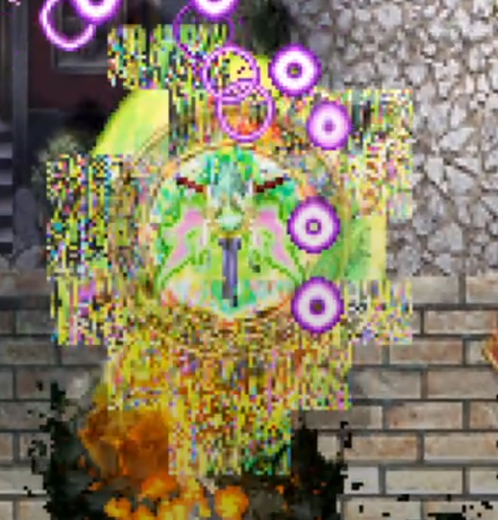
Basically, when I got it, the bomb sprite looked like this

Video of issue:
View: https://youtu.be/mwyrOH6RVz4
What's happening here is that some data on the NAND used for graphics assets has gone bad, and CV1K games don't do any handling of such failures, so the decompress of the asset fails and just produces garbage. Apparently NAND block failures are common on these IC's (see note in cv1k.cpp in mame).
A while ago, I reverse engineered how to read and write data from U2 by bitbanging through jtag (see: https://github.com/buffis/cv1k_research/tree/main/JTAG ), which means that fixing this should be possible through JTAG!
So this is how I did so.
- Step 1: Figure out which assets are bad
The first thing to do is to get a good U2 dump. Easiest is to get one from a mame romset. I have a spare PCB that I have actually dumped though!

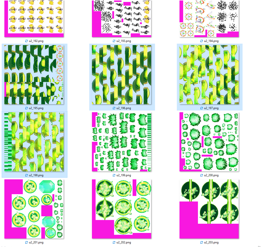
Then, since I reverse engineered the compression for assets, lets dump all the sprites for that and localize the bomb sprite. The command belows splits out PNG's for each asset.
https://github.com/buffis/cv1k_research/blob/main/U2_ExtractData/extract_gfx.py
Bomb sprites are in assets 195-198.

Then let's JTAG!
- Step 2: Figure out which block has those assets, and which one is bad
First, let's look at what bad blocks the device had from the factory. This looks at the bad block table of page1 of the NAND.
Ok, now lets get the full table of assets.
Now lets go to the second page of the NAND (offset 0x840) in the dump above. This has the table of assets. Go down 195 rows to find the assets we care about.
Each row is structured like this for assets:
As an example, asset #195 lives in block 0x3B, with an offset of 0x1D551 and a length of 0xB60D. All galuda2 assets are compressed.
Lets dump those assets. One block is 64 pages, so multiply block by 64 to get page counts.
Ok, so the asset positions using the table above are:
Let's extract those then:
Now, lets see if any of these doesnt decompress correctly (bad data). Use compress.py from U4_Tools in my repo:
Ok, so asset 197 is bad. That lives in block 0x3c-0x3d. Lets figure out WHERE it is bad.
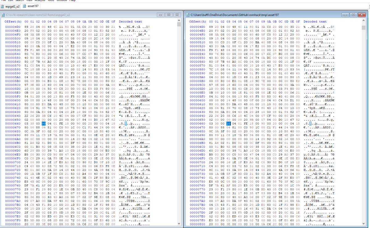
Open this in a hex editor and compare with original asset from clean dump:

Ok, so byte at offset 663 is incorrect. That is inside block 3C, so lets assume that block is now bad. Only assets 195 to 197 lives there.
- Step 3: Fix the assets
Ok, since the assets that touch that block might have issues, we need to write fresh copies of those somewhere else. There's two options here:
First step is to grab blocks 0x3B->0x3D into files (I called them galuda_3b, galuda_3c, galuda_3d). I just used a hex editor for this.
The new copies need to live after existing data on NAND, and last used one is:
...so lets write to 0x3dc ( 988 ) and onward which isn't used.
Ok, now we just need to update the mapping. We already have a dump from the PCB of the initial block, so time to modify that.
In block_0.dump now change byte 3-4 of each row to the new locations, since data uses same offsets:
This points the assets to the new addresses. This will look a bit weird in the table (like below), but work fine:
Finally, point the assets to their new addresses by overwriting the table on the NAND, and verify:
Then disconnected the JTAG, rebooted the game and hey, there we go!
View: https://youtu.be/rmWdcpjdUnw
This procedure should work for any other CV1000 game that has corrupted graphics due to bad NAND blocks. Use at your own risk, and only if you know what you are doing.
- Background
A while ago there was a Espgaluda 2 sold on YAJ that had sprite issues when bombing. https://page.auctions.yahoo.co.jp/jp/auction/x1005199728
I was looking at it, but price was a bit too high to me to justify getting it since I already have galuda2 on pcb, but the dude that ended up buying it agreed to send it to me to have a look at it, since I had a exciting idea for how to fix it using JTAG, without having to do any soldering!
Basically, when I got it, the bomb sprite looked like this
Video of issue:
What's happening here is that some data on the NAND used for graphics assets has gone bad, and CV1K games don't do any handling of such failures, so the decompress of the asset fails and just produces garbage. Apparently NAND block failures are common on these IC's (see note in cv1k.cpp in mame).
A while ago, I reverse engineered how to read and write data from U2 by bitbanging through jtag (see: https://github.com/buffis/cv1k_research/tree/main/JTAG ), which means that fixing this should be possible through JTAG!
So this is how I did so.
- Step 1: Figure out which assets are bad
The first thing to do is to get a good U2 dump. Easiest is to get one from a mame romset. I have a spare PCB that I have actually dumped though!
Then, since I reverse engineered the compression for assets, lets dump all the sprites for that and localize the bomb sprite. The command belows splits out PNG's for each asset.
https://github.com/buffis/cv1k_research/blob/main/U2_ExtractData/extract_gfx.py
Code:
> python3 extract_gfx.py good_u2Bomb sprites are in assets 195-198.
Then let's JTAG!
- Step 2: Figure out which block has those assets, and which one is bad
First, let's look at what bad blocks the device had from the factory. This looks at the bad block table of page1 of the NAND.
Code:
> sudo python3 K9F1G08U0M_JTAG.py bad_blocks
Starting
Resetting Flash
Reading page 0
Found bad blocks: [186, 187]
Done.
Ok, now lets get the full table of assets.
Code:
> sudo python3 K9F1G08U0M_JTAG.py read_all --filename=block_0.dump --page=0 --num_pages=64Now lets go to the second page of the NAND (offset 0x840) in the dump above. This has the table of assets. Go down 195 rows to find the assets we care about.
Code:
00001470: 0000 003b 0001 d551 0000 b60d 0200 0000  ...;...Q........       # <- Asset 195
00001480: 0000 003c 0000 7b5e 0000 e75b 0200 0000  ...<..{^...[....
00001490: 0000 003c 0001 62b9 0001 1b2a 0200 0000  ...<..b....*....
000014a0: 0000 003d 0000 6de3 0001 2fb4 0200 0000  ...=..m.../.....       # <- Asset 198
000014b0: 0000 003d 0001 9d97 0000 ccdd 0200 0000  ...=............       # <- Asset 199 (in same block as asset above)
Each row is structured like this for assets:
Code:
[ NAND block used ] - [ offset in block ] - [ num bytes of asset ] - [ compression type ]As an example, asset #195 lives in block 0x3B, with an offset of 0x1D551 and a length of 0xB60D. All galuda2 assets are compressed.
Lets dump those assets. One block is 64 pages, so multiply block by 64 to get page counts.
Code:
> sudo python3 K9F1G08U0M_JTAG.py read_all --filename=block59_to_61.dump --page=3776 --num_pages=192Ok, so the asset positions using the table above are:
Code:
195: Starts at: 0x1d551 , len 0xb60d
196: Starts at: 0x21000 + 0x7b5e , len 0xe75b
197: Starts at: 0x21000 + 0x162b9 , len 0x11b2a
198: Starts at: 0x21000 * 2 + 0x6de3 , len 0x12fb4
Let's extract those then:
Code:
dd skip=120145 count=46605 if=block59_to_61.dump of=asset195 bs=1
dd skip=166750 count=59227 if=block59_to_61.dump of=asset196 bs=1
dd skip=225977 count=72490 if=block59_to_61.dump of=asset197 bs=1
dd skip=298467 count=77748 if=block59_to_61.dump of=asset198 bs=1
Now, lets see if any of these doesnt decompress correctly (bad data). Use compress.py from U4_Tools in my repo:
Code:
> python3 compress.py asset195 195.out d
Size:  0x20014  Ops:  32011  Data offset:  0xfae
Wrote:  0x20014  expected:  0x20014


> python3 compress.py asset196 196.out d
Size:  0x20014  Ops:  42272  Data offset:  0x14b0
Wrote:  0x20014  expected:  0x20014


> python3 compress.py asset197 197.out d
Size:  0x20014  Ops:  53817  Data offset:  0x1a54
Traceback (most recent call last):
  File "compress.py", line 163, in <module>
    decompressed = decompress(infile.read())
  File "compress.py", line 54, in decompress
    out_data[out_ptr] = reused_data
IndexError: mmap index out of range


> python3 compress.py asset198 198.out d
Size:  0x20014  Ops:  58814  Data offset:  0x1cc4
Wrote:  0x20014  expected:  0x20014
Ok, so asset 197 is bad. That lives in block 0x3c-0x3d. Lets figure out WHERE it is bad.
Open this in a hex editor and compare with original asset from clean dump:
Ok, so byte at offset 663 is incorrect. That is inside block 3C, so lets assume that block is now bad. Only assets 195 to 197 lives there.
- Step 3: Fix the assets
Ok, since the assets that touch that block might have issues, we need to write fresh copies of those somewhere else. There's two options here:
- Mark the block as bad in the initial bad block table in page1, and move every asset after that block one block forward. Since NAND JTAG bitbanging is slow, this would take aproximately a week for write + verification.
- Just make another copy of the assets in the free space in the end, and change the initial table to use those. This takes less than an hour to write and verify. (this is what I did).
First step is to grab blocks 0x3B->0x3D into files (I called them galuda_3b, galuda_3c, galuda_3d). I just used a hex editor for this.
The new copies need to live after existing data on NAND, and last used one is:
Code:
000053a0: 0000 03da 0000 250d 0002 0014 0000 0000 ......%............so lets write to 0x3dc ( 988 ) and onward which isn't used.
Code:
pi@raspberrypi:~/github/cv1k_research/JTAG $ sudo python3 K9F1G08U0M_JTAG.py write_block --filename=galuda_3b --block=988
pi@raspberrypi:~/github/cv1k_research/JTAG $ sudo python3 K9F1G08U0M_JTAG.py write_block --filename=galuda_3c --block=989
pi@raspberrypi:~/github/cv1k_research/JTAG $ sudo python3 K9F1G08U0M_JTAG.py write_block --filename=galuda_3d --block=990

#Verify that writes worked:

pi@raspberrypi:~/github/cv1k_research/JTAG $ sudo python3 K9F1G08U0M_JTAG.py read_all --filename=block_988_verify.dump --page=63232 --num_pages=64
pi@raspberrypi:~/github/cv1k_research/JTAG $ sudo python3 K9F1G08U0M_JTAG.py read_all --filename=block_989_verify.dump --page=63296 --num_pages=64
pi@raspberrypi:~/github/cv1k_research/JTAG $ sudo python3 K9F1G08U0M_JTAG.py read_all --filename=block_990_verify.dump --page=63360 --num_pages=64

> crc32 gal* block_*
3b308f39        galuda_3b
d3f80267        galuda_3c
d3abd7d2        galuda_3d
3b308f39        block_988_verify.dump
d3f80267        block_989_verify.dump
d3abd7d2        block_990_verify.dump
Ok, now we just need to update the mapping. We already have a dump from the PCB of the initial block, so time to modify that.
In block_0.dump now change byte 3-4 of each row to the new locations, since data uses same offsets:
Code:
00001470: 0000 003b 0001 d551 0000 b60d 0200 0000  ...;...Q........       # <- 195
00001480: 0000 003c 0000 7b5e 0000 e75b 0200 0000  ...<..{^...[....
00001490: 0000 003c 0001 62b9 0001 1b2a 0200 0000  ...<..b....*....
to
00001470: 0000 03dc 0001 d551 0000 b60d 0200 0000  ...;...Q........       # <- 195
00001480: 0000 03dd 0000 7b5e 0000 e75b 0200 0000  ...<..{^...[....
00001490: 0000 03dd 0001 62b9 0001 1b2a 0200 0000  ...<..b....*....
This points the assets to the new addresses. This will look a bit weird in the table (like below), but work fine:
Code:
00001450: 0000 003b 0000 e59b 0000 7315 0200 0000  ...;......s.....
00001460: 0000 003b 0001 58b0 0000 7ca1 0200 0000  ...;..X...|.....
00001470: 0000 03dc 0001 d551 0000 b60d 0200 0000  ...;...Q........
00001480: 0000 03dd 0000 7b5e 0000 e75b 0200 0000  ...<..{^...[....
00001490: 0000 03dd 0001 62b9 0001 1b2a 0200 0000  ...<..b....*....
000014a0: 0000 003d 0000 6de3 0001 2fb4 0200 0000  ...=..m.../.....
000014b0: 0000 003d 0001 9d97 0000 ccdd 0200 0000  ...=............
000014c0: 0000 003e 0000 5a74 0000 d388 0200 0000  ...>..Zt........
Finally, point the assets to their new addresses by overwriting the table on the NAND, and verify:
Code:
> sudo python3 K9F1G08U0M_JTAG.py write_block --filename=block_0_fixed.dump --block=0
> sudo python3 K9F1G08U0M_JTAG.py read_all --filename=block_0_verify.dump --page=0 --num_pages=64
> crc32 block_0_fixed.dump block_0_verify.dump
d7ea01e8        block_0_fixed.dump
d7ea01e8        block_0_verify.dump
Then disconnected the JTAG, rebooted the game and hey, there we go!
This procedure should work for any other CV1000 game that has corrupted graphics due to bad NAND blocks. Use at your own risk, and only if you know what you are doing.


