mypinballs
Professional
Hi,
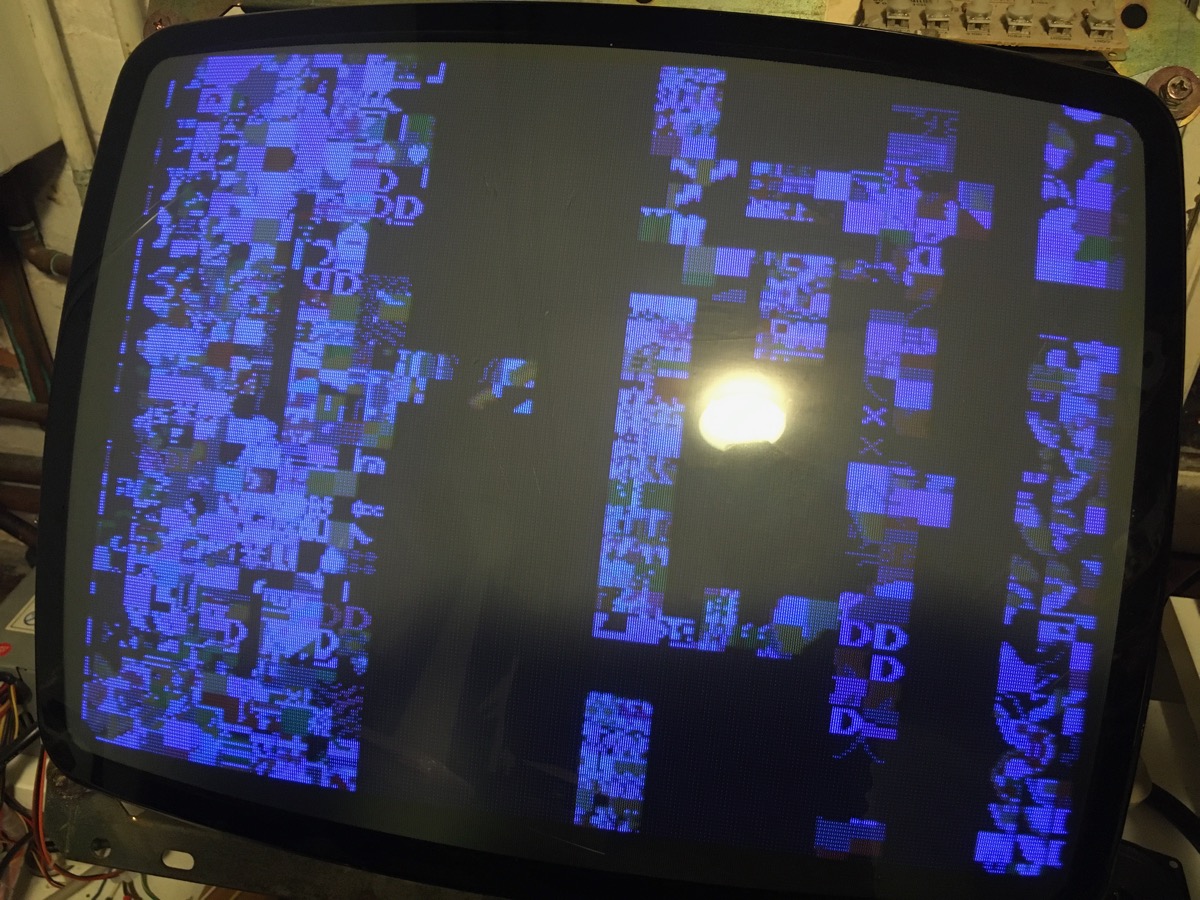
Have an original taito bubble bobble pcb that i got with a pile of random pcbs awhile back. I've started to look at. it's non working with just garbled graphics on screen.
First thing is the reset line is just resetting over and over (watchdog barking). Been looking at the schematics trying to fathom whats going on. I've tested the watchdog circuit itself and i can get it to stop resetting if i manually add a pulse at jp6 so that bit works.
I found a stuck high line at pin 5 ic39 which feeds the clk line to the ls273 at IC55. Changed that and no difference though i do see a pulse on that line now
Also have changed the z80 at ic50 and socketed (for high score save stuff later to), burned new roms (ic52, ic51, ic37, ic46) and new pal ics at ic49 and ic43. No different
Changed the work ram at IC44 (was a fujitsu ram and corroded), no different
Also changed ic35 as outputs looked alittle iffy, no different
I've checked all the usual things on the main z80. clock pulsing, rd and wr pulse (when not in reset), rfsh and mreq also look ok. Only thing i notice is the IORQ line on the z80 is high all the time.
Doe anyone know what is needed to get the main z80 out of reset and running, as it seems to be a loop on itself so i assume something is just making this cpu crash immediately.
Any help or pointers would be greatly received as its starting to do my head in!!!
Last edited:
