

Ape Cosplay
Grand Master
Yeah µPD4701s can be hard to source (altough you can find them in old serial mice at flea markets for $1), that's why a CPLD repro would be good.

Only ones I can find are suspect (from China). Going the EPM7128SQC100 route is tempting, but a bit more complicated than I want to undertake right now.Yeah µPD4701s can be hard to source (altough you can find them in old serial mice at flea markets for $1), that's why a CPLD repro would be good.
Dude thanks for this pinout, i'm a bit confused on this part:In that case just follow the diagram I posted above and replace the CPLD by a µPD4701:
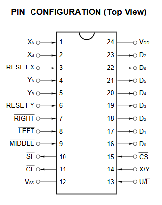
Wiring:
P2 UP (edge side) = pin 1 (Xa)
P2 DOWN (edge side) = pin 2 (Xb)
P2 LEFT (edge side) = pin 4 (Ya)
P2 RIGHT (edge side) = pin 5 (Yb)
CN4.7 = pins 3 (RESET X) & 6 (RESET Y)
CN4.6 = pin 14 (!X /Y)
P1 UP (board side) = pin 16 (D0)
P1 DOWN (board side) = pin 17 (D1)
P1 LEFT (board side) = pin 18 (D2)
P1 RIGHT (board side) = pin 19 (D3)
P1 A (board side) = pin 20 (D4)
P1 B (board side) = pin 21 (D5)
P1 C (board side) = pin 22 (D6)
P1 D (board side) = pin 23 (D7)
Lastly tie pins 13 (U/!L) and 15 (!CS) to ground.
(And don't forget the power pins OFC).
Now if you don't want to build a solution that would plug in place of a real SIT board disregard the edge side and simply wire the trackball directly to the µPD4701.
You'd need to amplify the signal coming from CN4.1, I can have a look at the transistor reference used on the original SIT board.
| Trackball | µPD4701 |
|---|---|
| X Clock | pin 1 (XA) |
| X Direction | pin 2 (XB) |
| Y Clock | pin 4 (YA) |
| Y Direction | pin 5 (YB) |
Pics always help.Hey,
What I meant is on the SIT board Xa for instance comes from P2 UP on the JAMMA (cab side).
You can totally wire the trackball directly to the 4701.
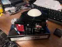
Maybe I should take a pic of the SIT board. On one side it connects to the JAMMA inside the cab, on the other side it connects to the JAMMA of the slot.
| Name | All | MV2F | MV1FZ* | SIT-IC-OUTPUT | Purpose |
|---|---|---|---|---|---|
| P1 Up | JAMMA 18 | 1P DB-15 Pin 15 | - | Trackball X / Y Bit 0 | 8-bit movement value |
| P1 Down | JAMMA 19 | 1P DB-15 Pin 7 | - | Trackball X / Y Bit 1 | 8-bit movement value |
| P1 Left | JAMMA 20 | 1P DB-15 Pin 14 | - | Trackball X / Y Bit 2 | 8-bit movement value |
| P1 Right | JAMMA 21 | 1P DB-15 Pin 6 | - | Trackball X / Y Bit 3 | 8-bit movement value |
| P1 Button A | JAMMA 22 | 1P DB-15 Pin 13 | - | Trackball X / Y Bit 4 | 8-bit movement value |
| P1 Button B | JAMMA 23 | 1P DB-15 Pin 5 | - | Trackball X / Y Bit 5 | 8-bit movement value |
| P1 Button C | JAMMA 24 | 1P DB-15 Pin 12 | - | Trackball X / Y Bit 6 | 8-bit movement value |
| P1 Button D | JAMMA 25 | 1P DB-15 Pin 4 | - | Trackball X / Y Bit 7 | 8-bit movement value |
| P2 Button A | JAMMA Z | 2P DB-15 Pin 13 | - | - | Left A |
| P2 Button B | JAMMA a | 2P DB-15 Pin 5 | - | - | Left B |
| P2 Button C | JAMMA b | 2P DB-15 Pin 12 | - | - | Right A |
| P2 Button D | JAMMA c | 2P DB-15 Pin 4 | - | - | Right B |
| Name | MV2F | MV1FZ* | SIT-IC-INPUT | Optional for trackball only? |
|---|---|---|---|---|
| P1 Output 1 | 1P DB-15 Pin 10 | NEO-D0 Pin 4 | Trackball X / Y select | No |
| P1 Output 2 | 1P DB-15 Pin 2 | NEO-D0 Pin 5 | Data | Yes |
| P1 Output 3 | 1P DB-15 Pin 9 | NEO-D0 Pin 6 | Clock | Yes |
| P2 Output 1 | 2P DB-15 Pin 10 | NEO-D0 Pin 7 | Latch | Yes |
| P2 Output 2 | 2P DB-15 Pin 2 | NEO-D0 Pin 8 | Card dispenser | Yes |
| P2 Output 3 | 2P DB-15 Pin 9 | NEO-D0 Pin 9 | Air Jet | Yes |
| Memory | Purpose | Source | Used by Irritating Maze |
|---|---|---|---|
| 0x10FE02 | Previous frame | 0x10FE03 | No |
| 0x10FE03 | Current frame | REG_P1CNT (0x300000) | No |
| 0x10FE04 | Delta (current - previous) | 0x10FE03 - 0x10FE02 | Yes |
| 0x10FE05 | Cache high 4 bit delta for direction | (0x10FE03 & 0xF0) - 0x10FE05 | No |
| Memory | Purpose | Structure | Source | Used by Irritating Maze |
|---|---|---|---|---|
| 0x10FD94[0-5] | "Joypad/Joystick state" | Bit 7 = P2 D Bit 6 = P2 C Bit 5 = P2 B Bit 4 = P2 A Bit 3 = X dir(+) Bit 2 = Y dir(-) Bit 1 = Y dir(+) Bit 0 = Y dir(-) | 7-4 = REG_P2CNT (0x340000)[BR]3-0 = BIOS calculation | No |
| 0x10FD9A[0-5] | "Joypad/Joystick state" | Same as above | Copy of 0x10FD94 | Yes |
| P2 Button A | JAMMA Z | 2P DB-15 Pin 13 | - | - | Left A |
| P2 Button B | JAMMA a | 2P DB-15 Pin 5 | - | - | Left B |
| P2 Button C | JAMMA b | 2P DB-15 Pin 12 | - | - | Right A |
| P2 Button D | JAMMA c | 2P DB-15 Pin 4 | - | - | Right B |


Talking this buttons, are they used in game ?
What is their purpose in the game?
it's to simplify wiring and maintenance even though they have the same function left and right by having independent wiring if one button fails it doesn't take out the other button and they can be independently tested in game test mode.Testing in game I understand that A is used but I don't understand what B is used for and why having two A and two B, I see that Left A and Right A in game do the same thing.
For the future trackball games of course!seems strange they would put it on the control panel if it's not used.
Not gonna lie, I was always surprised there wasn't a track ball enabled golf title at some point à la Golden Tee. Or League Bowling 2.For the future trackball games of course!
I'm trying to understand better the part about:
CN4.7 = pins 3 (RESET X) & 6 (RESET Y)
CN4.6 = pin 14 (!X /Y)

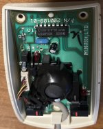
That'd be appreciated, having a hard time even finding pinouts for these things.If this uses the same technique as for reading a spinner then I now have a working circuit built using 74xx logic, obviously it needs to be doubled to read both the X and Y axis on a trackball or mouse.
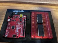
I did have a test sketch using an Arduino that would bit-bang a uPD4701 with a trackball attached to prove it worked. I'll see if I can find it.
I had since reinstalled my laptop so I had to dig through the backup I made before I wiped it. Here's what I found:That'd be appreciated, having a hard time even finding pinouts for these things.
// Basic NEC µPD4701AC test code
//
// Wire up the Arduino pins to the chip based on the comments below.
// You will use digital pins 2-11 as inputs and analog pins 0-4 as outputs.
//
// In addition:
// * Use 10KΩ pullup resistors on the three button inputs
// * Use 4.7KΩ pullup resistors on the four X1/X2/Y1/Y2 inputs

void setup() {
  Serial.begin(9600);

  // D0-D7
  pinMode(2, INPUT);
  pinMode(3, INPUT);
  pinMode(4, INPUT);
  pinMode(5, INPUT);
  pinMode(6, INPUT);
  pinMode(7, INPUT);
  pinMode(8, INPUT);
  pinMode(9, INPUT);

  // !SF
  pinMode(10, INPUT);

  // !CF
  pinMode(11, INPUT);

  // Reset X & Y
  pinMode(A0, OUTPUT);
  pinMode(A1, OUTPUT);
  digitalWrite(A0, LOW);
  digitalWrite(A1, LOW);

  // !CS
  pinMode(A2, OUTPUT);
  digitalWrite(A2, HIGH);

  // X/Y
  pinMode(A3, OUTPUT);
  digitalWrite(A3, LOW);

  // U/L
  pinMode(A4, OUTPUT);
  digitalWrite(A4, LOW);
}

byte readByte() {
  byte b;
  for (int i = 0; i < 8; i++) {
    b |= digitalRead(i+2) << i;
  }
  return b;
}

void loop() {
  byte left, middle, right;
  uint16_t x, y;

  // Read CF & SF interrupt pins
  if (!(digitalRead(10) && digitalRead(11))) {

    // CS low
    digitalWrite(A2, LOW);

    // X counter low byte (X/Y=0 U/L=0)
    digitalWrite(A3, LOW);
    digitalWrite(A4, LOW);
    x = readByte();

    // X counter high byte (X/Y=0 U/L=1)
    digitalWrite(A3, LOW);
    digitalWrite(A4, HIGH);
    x |= uint16_t(readByte()) << 8;

    // Pick out the button status from the upper nibble of the upper byte
    left = x & 0x4000 ? 1 : 0;
    right = x & 0x2000 ? 1 : 0;
    middle = x & 0x1000 ? 1 : 0;

    // Mask out the upper nibble of the upper byte
    x &= 0xfff;

    // Y counter low byte (X/Y=1 U/L=0)
    digitalWrite(A3, HIGH);
    digitalWrite(A4, LOW);
    y = readByte();

    // Y counter high byte (X/Y=1 U/L=1)
    digitalWrite(A3, HIGH);
    digitalWrite(A4, HIGH);
    y |= uint16_t(readByte() & 0xf) << 8; // Mask out the button status this time

    Serial.print("L=");
    Serial.print(left);
    Serial.print(" M=");
    Serial.print(middle);
    Serial.print(" R=");
    Serial.print(right);
    Serial.print(" X=");
    Serial.print(x);
    Serial.print(" Y=");
    Serial.println(y);

    // CS high again
    digitalWrite(A2, HIGH);
  }
}

