New Prog BK (Open Project)

pierpa86

Grand Master
Joined
May 5, 2022
Messages
711
Reaction score
1,011
Location
Italia
Hello Guys !
I made a project for fun, this is my first complicated PCB.
Goal is:
- P1 1MB + P2 4MB+ P3 4MB
- 4MB Vrom

For what i testing P part is working fine, CRC is OK !
Seems something wrong with V rom, its starting works but after a bit its start distorting sound.
Address conflict ?


edit: Working fine just make sure you have clean TSOP contacts and a working PCM.
The contacts are very small; check the solder connections carefully.
Using Goldfinger before sending to the manufacturer for printing costs a little more.

Since i dont want make money from that i will share with community.
I hope that with the help of the community we can make it better. ( for fun )
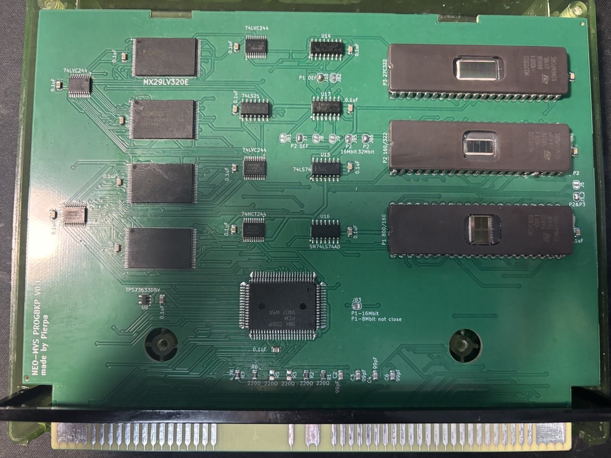
IMG_3412.JPG
 

Attachments

Last edited:
Great and interesting work!

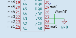
I believe there is a error in OE-pin since all memories cannot be active all the time.
Attached a reference from a KOF 97 prog board.

Edit: uploaded the whole prog-board pdf instead of a bad picture :)
 

Attachments

Great and interesting work!

I believe there is a error in OE-pin since all memories cannot be active all the time.
Attached a reference from a KOF 97 prog board.

Edit: uploaded the whole prog-board pdf instead of a bad picture :)
Thanks man,
But i connect CE and OE on 139 through LVC 244, on your PDF i see that CE is always enable on GND.
I dont get the error.:unsure:
 
Thanks man,
But i connect CE and OE on 139 through LVC 244, on your PDF i see that CE is always enable on GND.
I dont get the error.:unsure:
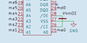
So the CE can be traced to ground no problem, but the OE must only be traced to the U7 74LVC244 in your case. To me it looks like it is also traced to ground which makes it shorted and therefor always low/active. You can try bending the pin up (be careful though, those are small pins :p) and then use a wire to U5/U7 directly to verify if that is the source.

If you measure the OE-pin to ground with a multimeter, it shouldn't read ~0 ohm, more like the pulled down value of something or OL. If that makes sense :)
 

Attachments

  • schematic_error.png
    schematic_error.png
    8.2 KB · Views: 21
So the CE can be traced to ground no problem, but the OE must only be traced to the U7 74LVC244 in your case. To me it looks like it is also traced to ground which makes it shorted and therefor always low/active. You can try bending the pin up (be careful though, those are small pins :p) and then use a wire to U5/U7 directly to verify if that is the source.

If you measure the OE-pin to ground with a multimeter, it shouldn't read ~0 ohm, more like the pulled down value of something or OL. If that makes sense :)
they are not on GND, they are both connected to LVC and 139

1773087035786.png
 
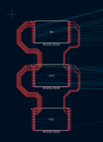
If nothing else pops up as the obvious fix, I would personally try to remove as many via:s as possible and try running address and data line close (but not to close) to each other like the attached example. This would improve two aspects, one is that the ground plane would be more solid and uniformed, but also via:s can cause EMF and make noise to close by traces. It is not a quick fix though.

Would love to see this project succeed so keep going! :)
 

Attachments

  • schematic_suggestion.png
    schematic_suggestion.png
    62.4 KB · Views: 28
The schematics in your zip don't match the pcb layout. The schematics say OE/CE should be tied to ground but your pcb layout has them going to the 244/139. Maybe you forgot to save the schematics before making the zip?
 
The schematics in your zip don't match the pcb layout. The schematics say OE/CE should be tied to ground but your pcb layout has them going to the 244/139. Maybe you forgot to save the schematics before making the zip?
Why you say that ?, there is no join point on GND:
If they are joined to GND should be like that:

1773096969192.png

But they are:
You have to see netlabel V2mOE

1773096986723.png
 
ah you are right. Its confusing having it like that, plus not having the V2m0E up against the pin makes it easier to misread.

The only thing that might be an issue, but probably not, is you might actually want the CE tied to ground. If you check the datasheet for MX29LV320E there are different timing for CE/OE for when the data pins become valid when they each go low.

I would be more suspect of a badly written vrom or installing them in the wrong locations. The vrom numbers aren't marked on the silk screen and they are in a non-standard order based on the OE nets

V3
V1
V2
V4

But overall good job on your first more complex board.
 
I unsoldered the first rom on top to check for broken memory.
Then, after checking integrity I have tested the board again to see if the problem persisted without that rom.
The ROM was fine and the game works.
So, I re-soldered the rom and after a while, I decided to clean the board's contacts on the comb side.
They were pre-tinned from the factory and aren't plated like the original board to improve contact.
So, in my opinion, that was the problem.
I leveled them to improve the surface and make it flat with the fiber optic pen, and I played for about 20 minutes, with no problems.
So, the board works. The game that i test was not funny but have 8MB of P2, perfect to test full P rom.
You're free to upgrade or use it. Enjoy as always
 
I unsoldered the first rom on top to check for broken memory.
Then, after checking integrity I have tested the board again to see if the problem persisted without that rom.
The ROM was fine and the game works.
So, I re-soldered the rom and after a while, I decided to clean the board's contacts on the comb side.
They were pre-tinned from the factory and aren't plated like the original board to improve contact.
So, in my opinion, that was the problem.
I leveled them to improve the surface and make it flat with the fiber optic pen, and I played for about 20 minutes, with no problems.
So, the board works. The game that i test was not funny but have 8MB of P2, perfect to test full P rom.
You're free to upgrade or use it. Enjoy as always
Great job!
Did you order it with "edge-connector" applied? Was always curious about what is actually ment more than a rounded edge. Maybe more flat pin surface as well? :)
 
It would also be interesting to use the definition of pcm 2 used in the vortex card instead of pcm1
https://github.com/neogeodev/NeoChips/tree/master/PCM
https://github.com/xvortex/VTXCart/tree/main/CPLD/MVS/PROG_PCM2

What do you suggest as candidates based on:
1) Unit price of the chip
2) Programmer price, program license
3) Availability on the market
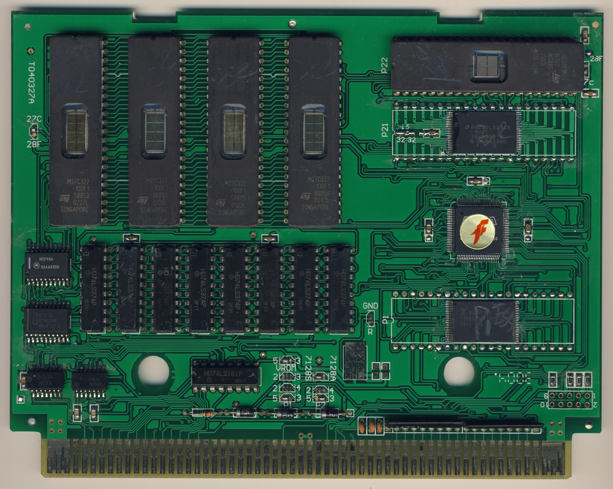
Well, I'm no expert by any means but I've seen it being made in two ways in bootlegs: a bunch of TTL or an altera max CPLD.
They used EPM7128SQC100, epm7128ati100, Epm7128elc84.
Kof2004_hero_special_bootleg1_b1_front.jpg
 
Last edited:
Back
Top