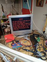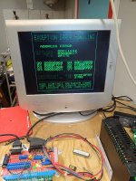

Got this board in a lot of three broken MV1F on eBay.
First issue to solve: no sync. Isolated and probed the sync pin on lspc-a2. No signal and the chip itself also got pretty warm. Put in a new chip and was greeted with a white screen.
All data- and adress lines on the system rom looked ok. Changed to uni-bios and got to a very corrupt looking crosshatch screen consisting of big, solid colored blocks.
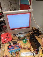
I could swap through the different menus. Noticed a blue color instead of green on the gradient screen. This made me suspect the ls273 chips and the resistors in the green-circuit. But when trying to boot a game the green color was there.
Speaking of games, cartridges did boot with uni-bios but no sound, sprites or text. Just ... Glitchiness.
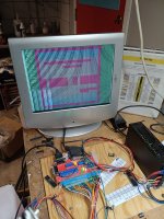
Probed randomly and decided to swap Neo b1 which was a speculative and stupid move. Got no change what so ever.
Probed lspc-a2. Found a short between pin 126 (p12) and ground. Fixed this and to my big relief p12 was still working. Still the same corrupt crosshatch though.
If only there were a fix layer so I could use the diag rom... Probed sfix-rom and noticed no activity on the adress pins. Looked at NEO-I0. The p-bus was working flawless but the Q-outputs to the sfix were dead. Changed NEO-I0 to a known working one.
Probed NEO-I0 again. Still dead outputs but this time I noticed that the PCK2B was low. Looked at neo dev wiki. This signal derives from an AS04 inverter. Both the input and the inverted output that is supposed to be the PCK2B were dead.
Traced the input side of the as04 to the NEO-B1 and got confused since I'd already put in a known working b1 there. Looked up the pin out on neo dev and this pin was registered as an input "PCK2"- not an output as I had assumed.
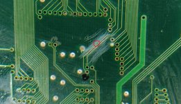
Traced the pin even more and sure enough, it derives from lspc-a2 and goes to neo-b1 (PCK2) but it also goes (in parallell) to the AS04 and then, as an inverted signal to neo-io as "PCK2B". Found and patched a rotten trace from the lspc-a2. Finally some.progress.
Now I booted to a cross hatch screen. Ran a game with uni-bios which played good except no sound.
Diagrom errored on no slot switch and then error code 4 - sound ram error.
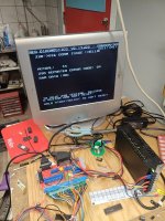
This turned out to be quite easy. The ram data pins looked suspicious on the oscilloscope so decided to trust the diagrom and changed the sound RAM.
This gave me the sound back and the satisfaction of bringing another beautiful NEO GEO back to life.
First issue to solve: no sync. Isolated and probed the sync pin on lspc-a2. No signal and the chip itself also got pretty warm. Put in a new chip and was greeted with a white screen.
All data- and adress lines on the system rom looked ok. Changed to uni-bios and got to a very corrupt looking crosshatch screen consisting of big, solid colored blocks.
I could swap through the different menus. Noticed a blue color instead of green on the gradient screen. This made me suspect the ls273 chips and the resistors in the green-circuit. But when trying to boot a game the green color was there.
Speaking of games, cartridges did boot with uni-bios but no sound, sprites or text. Just ... Glitchiness.
Probed randomly and decided to swap Neo b1 which was a speculative and stupid move. Got no change what so ever.
Probed lspc-a2. Found a short between pin 126 (p12) and ground. Fixed this and to my big relief p12 was still working. Still the same corrupt crosshatch though.
If only there were a fix layer so I could use the diag rom... Probed sfix-rom and noticed no activity on the adress pins. Looked at NEO-I0. The p-bus was working flawless but the Q-outputs to the sfix were dead. Changed NEO-I0 to a known working one.
Probed NEO-I0 again. Still dead outputs but this time I noticed that the PCK2B was low. Looked at neo dev wiki. This signal derives from an AS04 inverter. Both the input and the inverted output that is supposed to be the PCK2B were dead.
Traced the input side of the as04 to the NEO-B1 and got confused since I'd already put in a known working b1 there. Looked up the pin out on neo dev and this pin was registered as an input "PCK2"- not an output as I had assumed.
Traced the pin even more and sure enough, it derives from lspc-a2 and goes to neo-b1 (PCK2) but it also goes (in parallell) to the AS04 and then, as an inverted signal to neo-io as "PCK2B". Found and patched a rotten trace from the lspc-a2. Finally some.progress.
Now I booted to a cross hatch screen. Ran a game with uni-bios which played good except no sound.
Diagrom errored on no slot switch and then error code 4 - sound ram error.
This turned out to be quite easy. The ram data pins looked suspicious on the oscilloscope so decided to trust the diagrom and changed the sound RAM.
This gave me the sound back and the satisfaction of bringing another beautiful NEO GEO back to life.
Last edited: