Super street Fighter 2 garbled sprites

kissedin

Enthusiast
Joined
Jan 28, 2023
Messages
116
Reaction score
96
Location
Sweden
Ok. Before you write: I have tried a different a-board, yes I have 5V, Yes I have pressed down all Roms and pals in their sockets and yes I have made sure there is contact between A-B- and C-board.

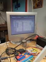
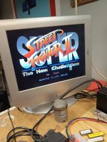
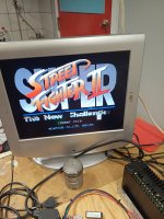
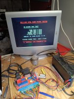
This board was working perfect the other day. Next day it looks like this: IMG_20260705_111558.jpg
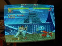
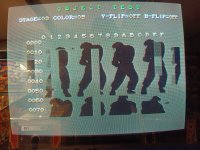
IMG_20260705_113459.jpg

All tests pass in in the self test. And all data and adress-lines are pulsing on the eprom with graphics (Roms 13-20).

It seems like an address issue but then, how come the Roms pass the self test? As you can see in the object viewer graphics are placed in the wrong places.

The board is equipped with an infinikeys that I haven't seen before if that should matter.IMG_20260705_174958.jpg
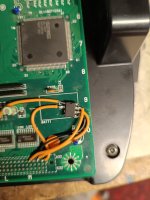
I know that there are excellent pinouts avaible but I would really like some help to where I should start looking. DL1827-CiF? Or any of the ls-series?

Board revision is 93646B-3
 
Small update. I was looking at neodev which said that sprites may be scattered if there is a problem with the higher adress lines. (Different systems I know but at least it was a clue.)

i found that b23 pin 2 and A23 pin 52 are low on the 2027 CGA chip. It is pulsing during startup but then Low Both of these pins are going to/from(?) the pal chip at 9h:bgsb3. So I want to replace it.

Does anyone know where there is a dump of this chip? Cannot find it anywhere.
 
Last edited:
It seems like an address issue but then, how come the Roms pass the self test? As you can see in the object viewer graphics are placed in the wrong places.
Self test only checks for main CPU program ROMs, not graphics or sound.

If you're lucky it's just a bad ROM, if a bit less lucky a logic chip or a bad trace, if really unlucky a custom chip.
 
Well, look at that. These are wonderful times to be living in.

I'll try to burn me a gal and see how it goes. CPS2 is new ground for me. Thank you so much for the link @ack
 
Self test only checks for main CPU program ROMs, not graphics or sound..
Yes I noticed that when half of the gfx Roms were out and the Rom test still said OK.
Lol :)

Unfortunately it is not the Roms. I pulled them out one by one but the glitch didn't change.

I still has to check every connection using the spreadsheet. Tidious work. I've probed all the customs except the security chip. They seemed ok. A pulsing Pin is not a guarantee that it's pulsing as it should though .mm

The only suspicious was the low a23 and b23 on the cga-chip.

Thank you for your advice @Ape Cosplay .
 
Update. Now I've burned the gal bgsb3. No change.

The good news is that the game boots and seem to function just the same as with the original chip. (It said status untested on the site)

Next Step will be to check continuity.
 
Last edited:
  • Like
Reactions: ack
I haven't checked all connections. It was working the other day when it was running for maybe 10 hours straight. Next day it played like it does now. Therefore I suspect one of the customs or a logic-chip. Specifically DL1927 which handles addresses.

Is there someone who got a ss2 and an oscilloscope or a probe and is willing to check pin 1 and pin 4 on the bgsb3 chip during gameplay?
 
I tried to replace the two other pals but no success.

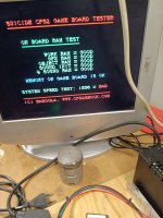
Then I tried Razoolas Suicide tester. All tests passed except the speed test. I turned up voltage to 5.1V which changed the status to "good". Same gfx glitches though.

IMG_20260719_231756.jpg

The problem is isolated to the object layer. I no longer sure it's an gfx adress issue. Because all the sprites CAN show up but some places in the object layer's grid are just blank and instead the sprites seem to show up at another place. Like this:
IMG_20260720_000312.jpg

For some reason "insert coin" can be displayed but not "free play"(only prints "fr Play" which is weird why can the latter e be displayed in "insert" but no in "free"?

IMG_20260719_233625.jpgIMG_20260719_232940.jpg


I'm not familiar with how the cps2 work. Now I'm about to give up. Or start shotgun troubleshoot the 5 customs. I have a xmen vs street Fighter that I reluctantly might sacrifice.

Which chip/circuit is responsible for mixing the graphics?

Is the onboard ram test reliable?
 
Last edited:
Do you get the same visual artefacts each time you boot the A+B board combo? If it's different then it might be worth looking closer at the RAM
 
It is the same each time. But I've done some further investigations and am leaning towards the object ram. Just ordered some replacement.

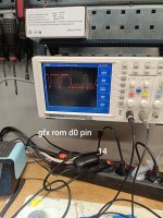
Checked the adres lines. They looked ok. The data lines however had brief moments when they look suspicious:

IMG_20260721_214731.jpg

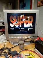
By plain curiosity I shorted two adjacent adress pins, A5 and A4 on the object ram at 4A, and noticed a change in the garbled sprites. Decided to lift A4.

With A4 lifted the object ram test still got an "OK" att the boot up. This was unexpected. Then I noticed that instead of "FR PLAY" the game showed " EE PLAY".

IMG_20260721_020210.jpg

Lifted I/O4 from the same ram chip. Now I got "object ram NG". Soldered same pin back to place. Still object ram NG. Soldered the adress pin back and all tests passed. Desoldered the adres pin again but ram test did pass at several boots. Complex behaviour.

I connected A4 when the game was running - and for a short period "FREE PLAY" was displayed. This made me suspect the RAMs (Fujitsu).

Edit: pin 6 is A4 in these rams (not a6).
 
Last edited:
It doesn't surprise me lifting the address still causes the games internal ram check to pass. It seems a number games just validate data in == data out for eac memory location. They don't consider that if there is a broken address line, 2 memory locations can get mapped to the same memory cell in the ram chip. I ran into this on a konami aliens board a while ago.

When you have the address pin lifted does the suicide tester see it as bad?
 
@ack now I've tested and the suicide ROM's test pass with A4 (pin 6) lifted on the object RAM at 4A.

Edit: rebooted the game. After this object ram test as bad.
Soldered back A4. Ran suicide test again: ram ok.

Lifted a4. Ran suicide test: ram ok.

Rebooted: ram test bad.
 
Last edited:
Here are the test results.

Edit: just realized that the RAMs on the b-board are the S-rams according to the wiring diagram. Sorry for any confusion.

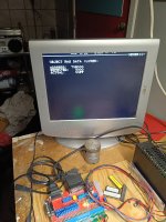
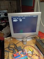
First try: a4 on S-RAM @4a desoldered.IMG_20260723_235228.jpg

Second, third and fourth try: all s-Ram pins attached.IMG_20260723_235452.jpg

And final try, same setup as in 2,3 and 4th try but now with Suicide tester:
IMG_20260724_000345.jpg

So it seems that the mad is doing a better job and you got something very precious cooking there :)
 
Last edited:
mad seems to think there is something wrong related to the object ram chip at 3A based on your 2nd screen shot.

If you want, you can try the attached version of mad. I have it set bypass normal startup checks and go directly to the menu system. If you go to the memory viewer then object ram, you can look around. I have memory debug built in for the memory viewer, which causes a long to get written to the first address displayed on the screen when you press the button 1. Each time you press button 1 the long will change by having each byte in the long increased by 1. ie: 0x00000000 -> 0x01010101 -> 0x02020202 etc.

I usually only use the memory debug stuff when probing around in a games address space to track down what is read/write ram, ram ranges and rams mirrors
 

Attachments

Thank you very much. I'll certainly try it. But why is it referred to as object ram when pinouts and wiring diagram say s-Ram? Or is it just me that is a bit drunk? Lol!
 
For the schematics if you trace it back he actually calls it OBJRAM. It just seems to be the links between the object ram and the DL-1827 that are referred to as SRAM.
 
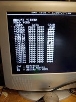
I've ran some ram tests. I suppose that there should all be "Ffff ffff" for all addresses.

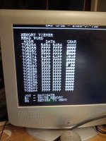
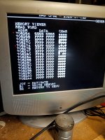
Some addresses weren't. I tried to write to these addresses. What happened is that another adress got changed as well. Video is to large to upload. But here are three pictures that describe what happens:

IMG_20260724_013421~2.jpg
First picture, address 708264 (marked with a red dot) is deviant. Address 708274 seem ok.

IMG_20260724_013502~2.jpg
Second picture, while trying to write to address 708264 address 708274 is also affected.

IMG_20260724_013523~2.jpg
Third picture, if I increase the number to be written to adress 708264, so will address 708274. But its only the upper byte (2 hex digits = 8 bits) that is increasing in each word (4 hex digits = 16 bits).

Please note that this also works the other way around. If I add to the address 708274 the two upper bytes will increase in adress 708264.

(I assume that each word has one byte from lower sram - and one byte from upper sram. But for some reason the upper sram "bleeds" data to certain intervened addresses.)

Edit: strikes me also that intervened addresses are for example:
7080A0 - 7080B0=16
708274- 708264=16

So always 16 away from each other for those addresses that are interevened. I don't know what this means. But I hope it means that it's just a ram :)
 
Last edited:
Back
Top