You are using an out of date browser. It may not display this or other websites correctly.
You should upgrade or use an alternative browser.
You should upgrade or use an alternative browser.
InfiniKey-CPS2
- Thread starter undamned
- Start date
XtraSmiley
Legendary
Yes, recently. He's fine, but I think has taken a little bit of a break from selling. He said parts to build more are still expensive, so I don't know what ETA on new things are.Has anyone heard from Undamned recently? I've been trying to contact him for several months, getting a little worried that something has happened to him
Follow him on Twitter if you want to see more from him.
skate323k137
Enlightened
I can't speak for the ICs in UDs products specifically, but right now if you have a product/project that relies on an IC that isn't in stock at a major supplier, you're all but screwed. This is a good read on the not great situation:
https://www.bigmessowires.com/2022/09/15/semiconductor-shortage-and-business-threat/
https://www.bigmessowires.com/2022/09/15/semiconductor-shortage-and-business-threat/
Raph_friend
Grand Master
Parts for USB2DB15 are really crazy expensive right now and worst part is that that's a pre-order from factory to get the main IC, and it takes almost one year on queue, hopefully i have plenty for a long run. Hope UD back to business soon.
skate323k137
Enlightened
A lot of chips say year plus lead times... I'll be surprised if a lot of them see another run at all. We can hope.
Stupid Dufus
Grand Master
https://www.twitter.com/therealundamnedWhat's his twitter address ?
Just talked to him yesterday. He is now moving to a new house and just doesn't have hobby time.
Okay guys, thanks for your patience. Here are the Gerber files for the PCBs (I used PCBWay with good results), and the hex files for the chips.
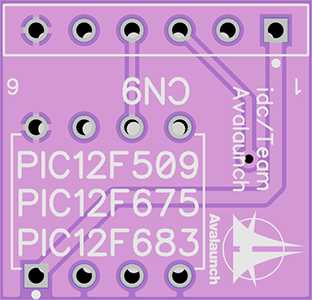
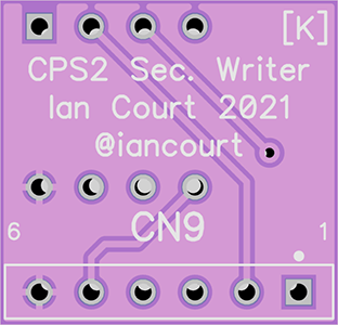
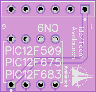
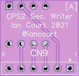
There are two PCB layouts:
You can use a suitable eight-pin DIP socket for the PICs, or you can just solder them straight in if you're not going to need to reprogram the chip at any point, or use the mod in another game board.
There are four groups of hex files:
I write the PICs with a GQ-4X programmer.
I think I have most, if not all, currently dumped games covered. Please let me know if you notice any that may be missing!
konosuke pinout PCB (note [K] marking in the silkscreen):


aje_fr pinout PCB (note [A] marking in the silkscreen):


There are two PCB layouts:
- idc-CPS2_PIC12F509_629_675_683_DIP_konosuke_pinout_v4_gerber.zip - this follows the same pinout as konosuke's excellent CPicS2 project
- idc-CPS2_PIC12F509_629_675_683_DIP_aje_fr_pinout_v4_gerber.zip - this follows the same pinout as aje_fr's chips
You can use a suitable eight-pin DIP socket for the PICs, or you can just solder them straight in if you're not going to need to reprogram the chip at any point, or use the mod in another game board.
There are four groups of hex files:
- PIC12F509_konosuke_pinout - compatible with PIC12F509 chips only, following konosuke's CPicS2 pinout
- PIC12F675_konosuke_pinout - compatible with PIC12F629, PIC12F675 and PIC12F683 chips, following konosuke's CPicS2 pinout
- PIC12F509_aje_fr_pinout - compatible with PIC12F509 chips only, following aje_fr's pinout
- PIC12F675_aje_fr_pinout - compatible with PIC12F629, PIC12F675 and PIC12F683 chips, following aje_fr's pinout
I write the PICs with a GQ-4X programmer.
I think I have most, if not all, currently dumped games covered. Please let me know if you notice any that may be missing!

Code:
konosuke pinout:                     aje_fr pinout:

           +---\/---+                            +---\/---+
   +5V:Vdd |1*     8| Vss:GND            +5V:Vdd |1*     8| Vss:GND
  DATA:GP5 |2      7|                   DATA:GP5 |2      7| GP0:SETUP2
SETUP1:GP4 |3      6| GP1:CLOCK                  |3      6| GP1:CLOCK
           |4      5| GP2:SETUP2                 |4      5| GP2:SETUP1
           +--------+                            +--------+


                          CPS2 CN9:

                           +---+
                           | 1*| +5V
                           | 2 | DATA
                           | 3 | SETUP1
                           | 4 | CLOCK
                           | 5 | SETUP2
                           | 6 | GND
                           +---+
konosuke pinout PCB (note [K] marking in the silkscreen):
aje_fr pinout PCB (note [A] marking in the silkscreen):
Attachments
Last edited:
I there a version for -3 and -4 pcbs?
I there a version for -3 and -4 pcbs?
Good question! I was going to look into it… I only went the PIC route as I had a load of old chips which used to use for PS1 mods and I wanted something to mess around with during the pandemic.
I would still consider doing a version for non-CN9 boards, but I’m not sure if there is much point. ack’s openkey solution seems to fit the bill rather nicely.

runfromcheese
New User
Am I correct to assume once a board is revived with an infinikey. If wanted to could I install a battery and remove the infinikey?
Yes. Install both the infinikey and the battery. Boot to set the key. Then power off and remove the infinikey.Am I correct to assume once a board is revived with an infinikey. If wanted to could I install a battery and remove the infinikey?
runfromcheese
New User
Thank you for the reply. Appreciate it.Yes. Install both the infinikey and the battery. Boot to set the key. Then power off and remove the infinikey.
tDRG
Grand Master
I picked up a board that hadn't been tested in a while. Battery (exp date 2014) hasn't exploded, but I get a forest green screen at bootup and the test menu doesn't work. Sound like a key issue, or something I need to debug before attempting an install?
duffcon
Professional
That sounds like a suicide. Usually the result is a single color screen. I would go with the key first, it can't hurt anything at this point.
Last edited:
tDRG
Grand Master
Kidkaos
Champion
Will they be $10 each again? Or still $20+ shipping??
AlxUnderBase
Enlightened
On the shop (paradisearcadeshop is listed with 20$ + shipping and on VGP is 19.64€ + shipping)Will they be $10 each again? Or still $20+ shipping??
