I can tell you that the PALs are somewhat related to the code on the GFX board too, or at least they share address lines and will get screwed up if the PAL is not functioning properly. when I was testing different things out I ended up corrupting JUST the sound by using the wrong PAL on the PRG board.If we are lucky we may not need a PAL at all, and get away with one or two 74lsXX. The MAME code doesn't suggest any complex banking or decoding.
You are using an out of date browser. It may not display this or other websites correctly.
You should upgrade or use an alternative browser.
You should upgrade or use an alternative browser.
Any PGM Conversion info out there?
- Thread starter 98pacecar
- Start date
A
Apocalypse
Having the equations and source pld file reversed allows you to rearrange pins as you like.knowing specifically which PCB revision they came from is important because I've discovered that the pin mapping is completely different for the same game even on different revisions of the same PCB. For instance PALS for KOV2 on 0333-01 PCB are pinned completely different than the PALS for KOV2 on the 0333-03 PCB
Cleraly, for instance the romboards for S16B/S18/S24 multis don't have the LS138/LS139 OG boards have (used to generate active low chip enable signals from higher address lines).If we are lucky we may not need a PAL at all, and get away with one or two 74lsXX. The MAME code doesn't suggest any complex banking or decoding.
That is interesting. The M-ROM data and address lines seemed to go directly to the sound chip, though it is possible that the sound code uses parts of the program board for obfuscation. Did it sound more like scrambled samples, or wrong sample start/end positions? Or wrong notes being played?I can tell you that the PALs are somewhat related to the code on the GFX board too, or at least they share address lines and will get screwed up if the PAL is not functioning properly. when I was testing different things out I ended up corrupting JUST the sound by using the wrong PAL on the PRG board.
Which PCB was this on and which game?
On my KOVSH board the inputs of EKU8 connect to the bus, the outputs to the T-ROM and to the enable of the built-in T-ROM. I haven't traced the bus connections on the motherboard, but I think they may address lines only. The wiring suggests that some obfuscation is possible with A18-A21 of the T-ROM, but I haven't noticed anything in MAME. What IS possible is that the address lines are ordered differently on different PCB versions, so that you can't swap this PAL between different PCBs.
EKU7 is only connected to the ASIC and the ROM. The inputs go to the ASIC, the output to program ROM enable and address lines. If the sound data is near the end of the ROM then wrong decoding of the higher address lines would corrupt it.
In any case, it should be possible to replace them with discrete logic once we know exactly what they do.
It was KOV2 running EspgaludaWhich PCB was this on and which game?
Indeed. Do you have a Killing Blade Cart? you could probably figure out how to get those working at ARM free PCB.Having the equations and source pld file reversed allows you to rearrange pins as you like.
Heck I'd love to know the equations just so I could make some dedicated GALs to replace the ones on my conversions with jumper wires and unsocketed pins.
A
Apocalypse
I only have a DoDonpachi convert (my Xmas gift from @lorenzo2marsIndeed. Do you have a Killing Blade Cart? you could probably figure out how to get those working at ARM free PCB.
Heck I'd love to know the equations just so I could make some dedicated GALs to replace the ones on my conversions with jumper wires and unsocketed pins.
 ).
).I'll publish the source pld files once tested.
My guess for EKU8:
- It takes TA18-TA23 from the connector
- It subtracts the base address for the ROM, 0x180000 in byte or 0xC0000 in words, from the high address lines and produces new address lines TA18-TA21 going to the T-ROM
- It checks if the address is in the 8MB range of the ROM and generates the OE signal for the built-in T-ROM on pin 19 and the cart T-ROM on pin 18
Update:
With a bit of python and a Quine-McCluskey solver I arrive at:
TA18_I = (NOT TA1
TA19_I = (((NOT TA1 AND TA19) OR (TA18 AND (NOT TA19)))
TA20_I = (((NOT TA19) AND (NOT TA20)) OR (TA18 AND TA19 AND TA20) OR ((NOT TA1 AND (NOT TA20)))
TA21_I = ((TA18 AND TA19 AND TA21) OR TA22 OR (TA20 AND TA21))
OE_CART = (((NOT TA19) AND (NOT TA20) AND (NOT TA21) AND (NOT TA22)) OR (TA18 AND TA19 AND TA22) OR TA23 OR (TA21 AND TA22) OR ((NOT TA1 AND (NOT TA20) AND (NOT TA21) AND (NOT TA22)) OR (TA20 AND TA22))
OE_INT = (TA22 OR TA21 OR (TA18 AND TA19) OR TA23 OR TA20)
... probably a bit much for discrete logic, but I have no idea how close my guess is to the real expression.
Update:
I resurrected my window xp machine to use my genius g540, only to find out it doesn't work with 27c322. Doh! To get at least some use out of it I tried to read the PAL from KOVSH:
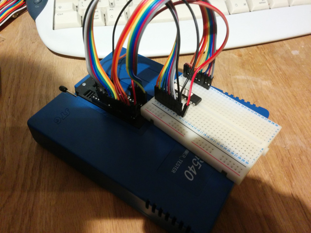
I took the pinout for a 28c16, connected the address lines to the inputs and the data lines to the output. The result are those two binary files in the zip.
Results:
EKU8 seems to work pretty much as predicted above. The only surprise is U8 pin 7/J2 pin 29: The enable lines are only generated when it is 1. This is strange, because if this is an address line I would expect it to be 0, as the tile roms are loaded to the start of the address space, if this was OE it would be 0 because enable is active low. Weird. Maybe I made a mistake reading it, though.
EKU7 subtracts 1 from A19/A20 and generates the enable lines for U1-U6: U1 and U3/U4 are enabled for output 0, U1 and U4/U5 are enabled for output 1, U1 and U2 are enabled for output 2. Interestingly 3 doesn't seem to be decoded? Any input lower than 1 or higher than 3 disables all OE.
ASIC 5 and 4 seem to be A19 and A20, I guess ASIC 3 and 2 are A21 and A22.
- It takes TA18-TA23 from the connector
- It subtracts the base address for the ROM, 0x180000 in byte or 0xC0000 in words, from the high address lines and produces new address lines TA18-TA21 going to the T-ROM
- It checks if the address is in the 8MB range of the ROM and generates the OE signal for the built-in T-ROM on pin 19 and the cart T-ROM on pin 18
Update:
With a bit of python and a Quine-McCluskey solver I arrive at:
TA18_I = (NOT TA1

TA19_I = (((NOT TA1
 AND TA19) OR (TA18 AND (NOT TA19)))
TA20_I = (((NOT TA19) AND (NOT TA20)) OR (TA18 AND TA19 AND TA20) OR ((NOT TA1
 AND (NOT TA20)))
TA21_I = ((TA18 AND TA19 AND TA21) OR TA22 OR (TA20 AND TA21))
OE_CART = (((NOT TA19) AND (NOT TA20) AND (NOT TA21) AND (NOT TA22)) OR (TA18 AND TA19 AND TA22) OR TA23 OR (TA21 AND TA22) OR ((NOT TA1
 AND (NOT TA20) AND (NOT TA21) AND (NOT TA22)) OR (TA20 AND TA22))
OE_INT = (TA22 OR TA21 OR (TA18 AND TA19) OR TA23 OR TA20)
... probably a bit much for discrete logic, but I have no idea how close my guess is to the real expression.

Update:
I resurrected my window xp machine to use my genius g540, only to find out it doesn't work with 27c322. Doh! To get at least some use out of it I tried to read the PAL from KOVSH:
I took the pinout for a 28c16, connected the address lines to the inputs and the data lines to the output. The result are those two binary files in the zip.
Results:
EKU8 seems to work pretty much as predicted above. The only surprise is U8 pin 7/J2 pin 29: The enable lines are only generated when it is 1. This is strange, because if this is an address line I would expect it to be 0, as the tile roms are loaded to the start of the address space, if this was OE it would be 0 because enable is active low. Weird. Maybe I made a mistake reading it, though.
EKU7 subtracts 1 from A19/A20 and generates the enable lines for U1-U6: U1 and U3/U4 are enabled for output 0, U1 and U4/U5 are enabled for output 1, U1 and U2 are enabled for output 2. Interestingly 3 doesn't seem to be decoded? Any input lower than 1 or higher than 3 disables all OE.
ASIC 5 and 4 seem to be A19 and A20, I guess ASIC 3 and 2 are A21 and A22.
Attachments
Last edited:
Look what the postman brought today! Yes, I went for red:
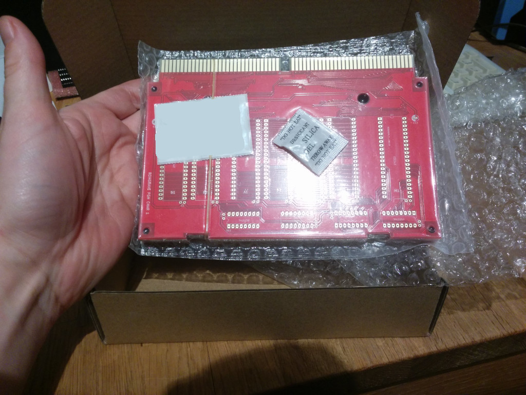
(One reason is because that seems to be the main colour used for PGM, and the other is so that they are easily identifiable in an eBay picture. )
)
A quick prototype fit:
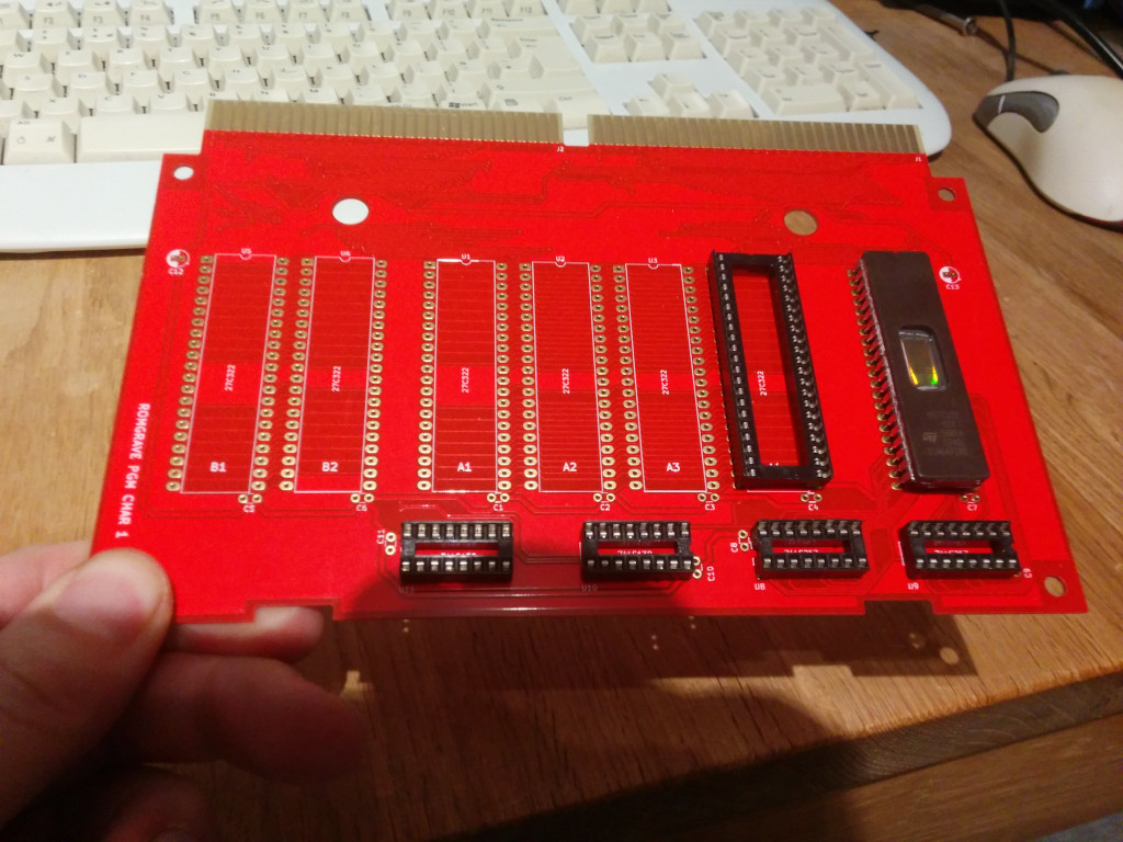
I don't have time until Saturday to put it together and test one. I'll make one with sockets, once I'm happy that it works I'll make one with the chips directly soldered in.
A bit of a tight fit on the sides, I may have to shave of a bit of the pcb size if I make another order:
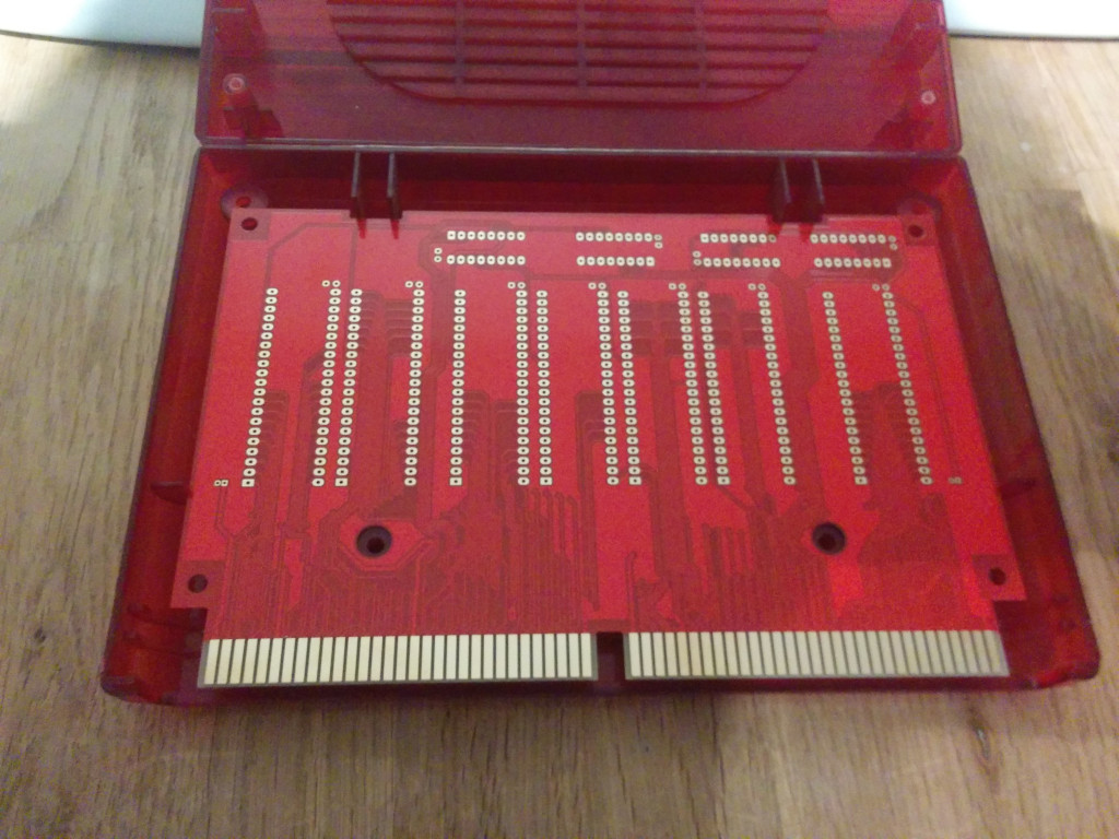
The holes seem to fit perfectly, the cartridge closes nicely.
Fits into the slot:
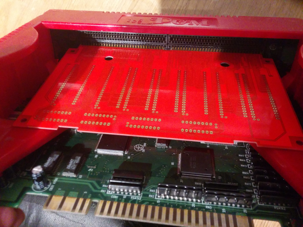
Small update for the prog board:
It looks like the m68k bus is a bit more complicated than 8-bit processors: http://research.cs.tamu.edu/prism/lectures/mbsd/mbsd_l15.pdf
There is either the AS+DTACK asynchronous protocol, or the VPA+VMA synchronous protocol. I was able to trace AS to the connector, if we can work out how DTACK can be generated we can read unencrypted ROMs.
(One reason is because that seems to be the main colour used for PGM, and the other is so that they are easily identifiable in an eBay picture.
 )
)A quick prototype fit:
I don't have time until Saturday to put it together and test one. I'll make one with sockets, once I'm happy that it works I'll make one with the chips directly soldered in.
A bit of a tight fit on the sides, I may have to shave of a bit of the pcb size if I make another order:
The holes seem to fit perfectly, the cartridge closes nicely.
Fits into the slot:
Small update for the prog board:
It looks like the m68k bus is a bit more complicated than 8-bit processors: http://research.cs.tamu.edu/prism/lectures/mbsd/mbsd_l15.pdf
There is either the AS+DTACK asynchronous protocol, or the VPA+VMA synchronous protocol. I was able to trace AS to the connector, if we can work out how DTACK can be generated we can read unencrypted ROMs.
A
Apocalypse
Very nice work @Fluffy.
I haven't got time to check but according to my notes about EK7:
o14 = !i5;
o15 = !(i4 $ i5);
o16 = !i2 & !i3 # i4 # i5;
o17 = i2 # i3 # !i4 # !i5;
o18 = i2 # i3 # !i4 # i5;
o19 = i2 # i3 # i4 # !i5;
ix = input pin x
ox = output pin x
Target device = GAL16V8
[EDIT]
Might try the reversed EK7 and EK8 during the weekend.
Last edited by a moderator:
Just to answer a few questions:
I got the PCBs manufactured with https://jlcpcb.com/e .
I looked at pcbway as well, but jlcpcb had an offer on shipping. I'm sure most pcb houses can produce these boards at similar quality levels (if they aren't reselling each other's services in the first place. )
)
Yes, at some point I'll have PCBs available for share. I'll have to be sure that they work, first.
I don't plan a multi: I don't have time to patch all games to run without ASIC, and bigger flash chips come only in surface mount packaging which I don't really want to hand solder. You can get PCBs made together with assembly, but that'll be a bigger investment in time and money. If someone else wants to do it they are welcome, though!
This is the latest version of the KOVSH schematic. I think the graphics board should be complete, the last change was to replace A_ROM_ENABLE with AA24, as AA22-24 are used as an input into a 74ls138 on a PCB334-00. There is a lot of speculation on the program board, and I need to check some non-connected cartridge pins against a higher capacity cart to see what they are.
I got the PCBs manufactured with https://jlcpcb.com/e .
I looked at pcbway as well, but jlcpcb had an offer on shipping. I'm sure most pcb houses can produce these boards at similar quality levels (if they aren't reselling each other's services in the first place.
 )
)Yes, at some point I'll have PCBs available for share. I'll have to be sure that they work, first.
I don't plan a multi: I don't have time to patch all games to run without ASIC, and bigger flash chips come only in surface mount packaging which I don't really want to hand solder. You can get PCBs made together with assembly, but that'll be a bigger investment in time and money. If someone else wants to do it they are welcome, though!
This is the latest version of the KOVSH schematic. I think the graphics board should be complete, the last change was to replace A_ROM_ENABLE with AA24, as AA22-24 are used as an input into a 74ls138 on a PCB334-00. There is a lot of speculation on the program board, and I need to check some non-connected cartridge pins against a higher capacity cart to see what they are.
Attachments
Last edited:
xodaraP
Legendary
I looked at JLC previously but hadn't heard any feedback so I wasn't sure, good to hear they're alright.
PCBWay is great but it's always good to have options. JLC seemed to be cheaper for multi layer stuff.
PCBWay is great but it's always good to have options. JLC seemed to be cheaper for multi layer stuff.
A
Apocalypse
Better than that, JLC is way cheaper for everything.JLC seemed to be cheaper for multi layer stuff.
edwin128
Student
I got a pgm and some carts for sale 

A
Apocalypse
U7 and U8 successfully reversed in GAL16V8 devices!
http://www.filedropper.com/pgmcartu7
http://www.filedropper.com/pgmcartu8
I haven't optimised equations for U8 yet but WinCUPL seems happy with them as they fit anyway.
[EDIT]
Couldn't find PLD file with reduced equations for U7...
So here are brute forced files (WinCUPL format):
http://www.filedropper.com/pgmcartu7
http://www.filedropper.com/pgmcartu8
I haven't optimised equations for U8 yet but WinCUPL seems happy with them as they fit anyway.
[EDIT]
Couldn't find PLD file with reduced equations for U7...
So here are brute forced files (WinCUPL format):
Apocalypse said:Name PGM_CART_U7;
Partno PAL_CE;
Revision 01;
Date 01/01/2017;
Designer Apocalypse;
Company None;
Location None;
Assembly None;
Device g16v8;
/****************************************************************/
/* */
/* General File Comments */
/* */
/****************************************************************/
/*
* Inputs: define inputs in this section
*/
Pin 2 = i2;
Pin 3 = i3;
Pin 4 = i4;
Pin 5 = i5;
/*
* Outputs: define outputs as active HI levels in this section
*/
Pin 19 = o19;
Pin 18 = o18;
Pin 17 = o17;
Pin 16 = o16;
Pin 15 = o15;
Pin 14 = o14;
/*
* Logic: logic equations in this section
*/
!o19 = !i2 & !i3 & !i4 & i5;
!o18 = !i2 & !i3 & i4 & !i5;
!o17 = !i2 & !i3 & i4 & i5;
!o16 = !i2 & !i3 & i4 & !i5
# !i2 & !i3 & !i4 & i5
# !i2 & !i3 & i4 & i5;
!o15 = i4 & !i5
# !i4 & i5;
!o14 = i5;
Apocalypse said:Name PGM_CART_U8;
Partno PAL_CE;
Revision 01;
Date 01/01/2017;
Designer Apocalypse;
Company None;
Location None;
Assembly None;
Device g16v8;
/****************************************************************/
/* */
/* General File Comments */
/* */
/****************************************************************//*
* Inputs: define inputs in this section
*/
Pin 2 = i2;
Pin 3 = i3;
Pin 4 = i4;
Pin 5 = i5;
Pin 6 = i6;
Pin 7 = i7;
/*
* Outputs: define outputs as active HI levels in this section
*/
Pin 19 = o19;
Pin 18 = o18;
Pin 15 = o15;
Pin 14 = o14;
Pin 13 = o13;
Pin 12 = o12;
/*
* Logic: logic equations in this section
*/
!o19 = !i2 & !i3 & !i4 & !i5 & !i6 & i7
# i2 & !i3 & !i4 & !i5 & !i6 & i7
# !i2 & i3 & !i4 & !i5 & !i6 & i7;
!o18 = i2 & i3 & !i4 & !i5 & !i6 & i7
# !i2 & !i3 & i4 & !i5 & !i6 & i7
# i2 & !i3 & i4 & !i5 & !i6 & i7
# !i2 & i3 & i4 & !i5 & !i6 & i7
# i2 & i3 & i4 & !i5 & !i6 & i7
# !i2 & !i3 & !i4 & i5 & !i6 & i7
# i2 & !i3 & !i4 & i5 & !i6 & i7
# !i2 & i3 & !i4 & i5 & !i6 & i7
# i2 & i3 & !i4 & i5 & !i6 & i7
# !i2 & !i3 & i4 & i5 & !i6 & i7
# i2 & !i3 & i4 & i5 & !i6 & i7
# !i2 & i3 & i4 & i5 & !i6 & i7
# i2 & i3 & i4 & i5 & !i6 & i7
# !i2 & !i3 & !i4 & !i5 & i6 & i7
# i2 & !i3 & !i4 & !i5 & i6 & i7
# !i2 & i3 & !i4 & !i5 & i6 & i7;
!o15 = i2;
!o14 = !i2 & !i3
# i2 & i3;
!o13 = i2 & i3 & !i4
# !i2 & !i3 & i4
# i2 & !i3 & i4
# !i2 & i3 & i4;
!o12 = i2 & i3 & !i4 & !i5
# !i2 & !i3 & i4 & !i5
# i2 & !i3 & i4 & !i5
# !i2 & i3 & i4 & !i5
# i2 & i3 & i4 & !i5
# !i2 & !i3 & !i4 & i5
# i2 & !i3 & !i4 & i5
# !i2 & i3 & !i4 & i5;
Last edited by a moderator:
which PCB number is that for?
EDIT, nevermind looking at photos those are used on IGS PCB No-0257-1
EDIT, nevermind looking at photos those are used on IGS PCB No-0257-1
Last edited:
A
Apocalypse
Those using EK7 & EK8 PAL chips.which PCB number is that for?
First results: No short circuits, the footprint for the ceramic capacitors is a bit small (fixed in next revision), the cartridge will not close with sockets installed (as expected). Now I just need to wait for my new EPROM programmer to arrive from China...
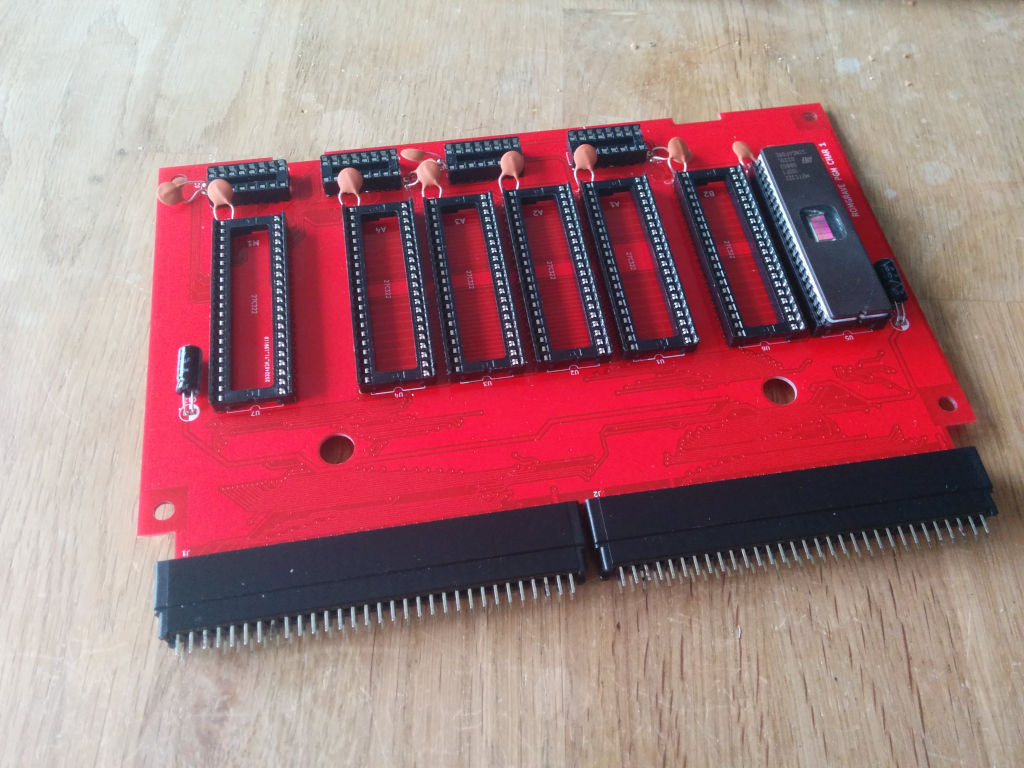
xodaraP
Legendary
I am definitely going to make them available, but I don't know in what form, yet.@Fluffy
Will you be selling these? I'd love to be able to make a couple of repro games and this would make things a lot easier
By the way, I attached my progress on 0333-03-FI. It matches what @twistedsymphony found with 0333-01.
I am convinced that the program PAL is reprogrammed or replaced in the ASIC-less conversion, otherwise I can't see how you get the correct mapping. Just to confirm (I am too lazy to go back through the thread): Ketsui and Espgaluda boot directly into the game, and not into the BIOS? Is that the same for the version with and without ASIC?
I'll try to dump the PAL tomorrow. There is a chance that the DTACK circuit uses a small state machine, in that case I don't think I can easily dump it.
Has anyone peeled of the stickers of the PALs on the KOV2 board?
Update: Pulled the chips, the silkscreen says "22V10".
Attachments
Last edited:
I needed a slightly different jig to read the 22V10:
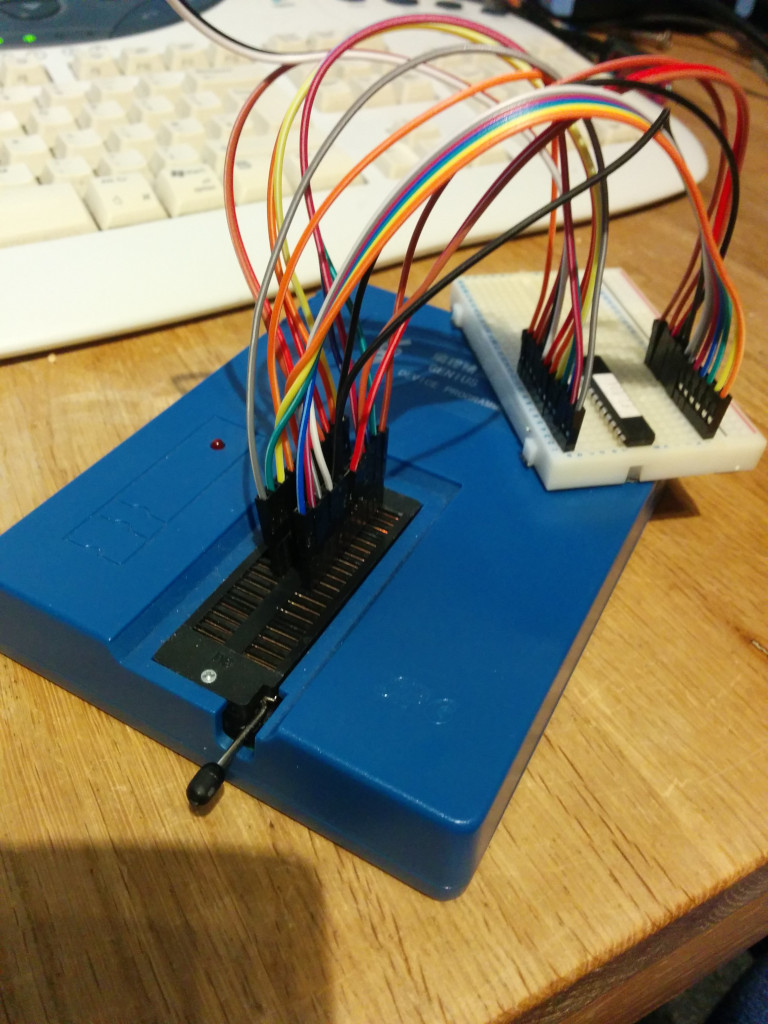
This uses a 32kb EPROM pinout as a base, and I had to read them in two passes to get all 10 output bits.
My computer then spent the rest of the day crunching the data and generating the pld files.
The zip file includes:
fi_u14.pld: the generated equations for U14, controlling mostly the tile-rom mapping.
fi_u14.si: the dumped data converted into a test vector, that way I can match the simulation with the generated equations.
PGM_FI_U14.jed: the pld file compiled with WinCUPL
fi_u15.pld: the generated equations for U15, controlling mostly the program-rom mapping
fi_u15.si: the dumped data converted into a test vector
PGM_FI_U15.jed: the pld compiled with WinCUPL
fi_u15_hack.pld: fi_u15.pld with the mod from Any PGM Conversion info out there? already applied:
- it assumes PA21 is permanently one
- it passes PA20 through unchanged
- it sets the ROM's pin 32 to permanently 0
PGM_FI_U15_HACK.jed: The pld compiled with WinCUPL
I didn't order any PALs with my last component order and I don't have any around, so if someone has the equipment please give it try. First try fi_u14 + fi_u15 if they work as a drop-in replacement for KOV2/Board 0333-03, then try if fi_u15_hack boots Ketsui/Espgaluda without modifications to the PAL wiring.
I noticed both PAL do some "extra" work in addition to handling ROM mapping which I haven't completely decoded, yet.
Attachments
Last edited:
