What's new
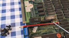
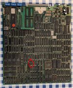
I am not sure what variant you have, especially since the program roms are the things that are missing. I can't find a 1:1 match between this and something dumped but you can go through the files and see if any of the labels & locations match perfectly. You need the 'main cpu' code burned onto chips on that sub-board. so perhaps this one https://github.com/mamedev/mame/blo...3cfdabb47205/src/mame/drivers/cps1.cpp#L10507 is a decent place to start if you're just winging it. to figure out which type of eproms to use you check the filesize on disc or in mame, confirm the pin count, and if you're stuck between multiple types you have to figure out where 5v and ground are and compare to the chips pinouts. that usually will tell you which variant is suitable. You're probably in need of two of each from this table but the pinout is going to tell you which one(s). Or four of the larger size, but doubling the binary so the code fills the chip.

1645550122523.png

It won’t boot without 5v that’s true. But you need to have programmed all main cpu roms on the appropriately sized and pinned chips as well. Did you find right sized and pinned chips? You said you only had 27c2001’s which are only valid for 2mbit data, and all the variants I see use at least 2x4mbit as well
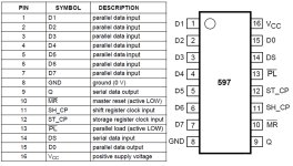
Here's my attempt at trying to make the pinout of the daughterboard easy to understand.
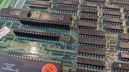
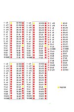
I haven't really studied it in detail yet myself, but if anyone can see what's going on here then please let me know.
In the meantime I'll try and make it easier to read.
 

Attachments

  • daughterboard.jpg
    daughterboard.jpg
    235.4 KB · Views: 96
Last edited:
Sorry for the length and grammar of the post ... :P

Ok, First, check in continuity mode if VCC is VCC and if GND is GND, in some boards the resistance is so low beetwen GND and 5v the multimeter gives beep beetwen the 2.
Ex. pin 31 and 12 on the 42 pin shoud be GND and you have VCC on 31.
In the 42 pin:
1-10 are addres lines - OK
11 is /E (chip enable) and goes to ls139 - OK
12 is GND - OK
13 in /G (output enable) and goes to pin 24 (/OE) of the other sockets - OK
14 to 21 are datalines - OK
22 is VCC - OK
23 - 29 datalines - OK
30 GND ..... should be D15/A-1 but problably dont use it
31 VCC ..... should be GND !!!
32-41 address lines - OK
42 if not used this gives you a clue. *** EDIT *** Ok, it uses to send info to ls139

The most used 42 pin epproms with that type of pinout are 27c800 / 27c160 / 27c322 and 27c800 is the only one not using pin 42 (and the smallest of the 3 with enough space for the cpu roms).
Problably the pinout for the 42 is a 27c800 / 27c160 / 27c322 (compatible pinouts)
Now the important, the pinout for the sockets.
You have to think it will be 27c010 / 27c020 or 27c040 (becouse of the size) and for that you have to search for the diferences.
The pinout are the same with the exception of pins 30 and 31.
27c010 dont use pin 30 and uses pin 31 for programming
27c020 uses pin 30 for addres (A17) but uses 31 for programming
27c040 uses pin 30 and 31 for address (A17 and A18 )

You have to check if the sockets have that lines going anywere, and then you will have the eproms needed for the CPU ROM.

Good luck!
 
Last edited:
Sorry for the length and grammar of the post ... :P

Ok, First, check in continuity mode if VCC is VCC and if GND is GND, in some boards the resistance is so low beetwen GND and 5v the multimeter gives beep beetwen the 2.
Ex. pin 31 and 12 on the 42 pin shoud be GND and you have VCC on 31.
In the 42 pin:
1-10 are addres lines - OK
11 is /E (chip enable) and goes to ls139 - OK
12 is GND - OK
13 in /G (output enable) and goes to pin 24 (/OE) of the other sockets - OK
14 to 21 are datalines - OK
22 is VCC - OK
23 - 29 datalines - OK
30 GND ..... should be D15/A-1 but problably dont use it
31 VCC ..... should be GND !!!
32-41 address lines - OK
42 if not used this gives you a clue.

The most used 42 pin epproms with that type of pinout are 27c800 / 27c160 / 27c322 and 27c800 is the only one not using pin 42 (and the smallest of the 3 with enough space for the cpu roms).
Problably the pinout for the 42 is a 27c800 / 27c160 / 27c322 (compatible pinouts)
Now the important, the pinout for the sockets.
You have to think it will be 27c010 / 27c020 or 27c040 (becouse of the size) and for that you have to search for the diferences.
The pinout are the same with the exception of pins 30 and 31.
27c010 dont use pin 30 and uses pin 31 for programming
27c020 uses pin 30 for addres (A17) but uses 31 for programming
27c040 uses pin 30 and 31 for address (A17 and A18 )

You have to check if the sockets have that lines going anywere, and then you will have the eproms needed for the CPU ROM.

Good luck!
Thanks, Apologies! I updated the image recently after finding some errors. I'll check your points against my new image though. Feels like progress.
 
The 2 right sockets have pin 22 (chip enable) tied to ls139 that only enables the eprom when needed. It have pin 24 (output enable) tied to the output enable ot the 42 pin.
They have pins 30 and 31 tied to addresses, and with the rest of the datalines and addresses I´m convinced the 2 right sockets are for 27c040.
Now lets look at the left sockets, check continuity with the right sockets (1 to 1, 2 to 2, 3 to 3 .....) and see if they have diferences and were goes pins 22, 24, 30 and 31.
 
I've updated the daughterboard pin mapping image (previous post) hopefully it's nearly there now as that really made my head hurt!!!
 
I think the pcb version is this one:
sf2mkot
Search in the board if you have the following ics in that possition.
gal16v8a or pal
u95, u96, u107, u125, u139, u151, u173, u176, u177, .u178, u183, u198, u218
gal20v8a or pal
u20, u21, u34, u35, u39, u104, u131, u135, u140
gal22v10-25lp or pal
u134
 
I think the pcb version is this one:
sf2mkot
Search in the board if you have the following ics in that possition.
gal16v8a or pal
u95, u96, u107, u125, u139, u151, u173, u176, u177, .u178, u183, u198, u218
gal20v8a or pal
u20, u21, u34, u35, u39, u104, u131, u135, u140
gal22v10-25lp or pal
u134
Thanks for this info that's an interesting way of identifying the version on the board. Where did you get the chip locations from?
I'm not matching the list but it's very close!
I have the GAL20v8a in the following locations:
U20
U21
U104
U131
U135
U140

The following are missing from the board:
U034
U035
U039

Thanks.
 
OK, close enough. They are only a few candidates. In the mame section of the driver's for the sf2 https://github.com/mamedev/mame/blob/master/src/mame/drivers/cps1.cpp search for a version with the same layout, 4 cpu roms, 8 gfx roms, 2 sound roms (1 cpu + 1 samples) and 1 unknown (user1).
Reading the notes from the 05/13/92 MSTREET-6 on cps1.cpp I think it has to be related to this version which was mentioned earlier in the posts.

I have the same sound chips:
YM2151 is clone marked "KA51"
YM3012 is clone marked "KA12".
MSM6295 is clone marked "TD735".

Also the same fault prone chip mentioned here:
Frequent cause of dead board is u104 (gal/palce20v8) becoming corrupted somehow.

But I don't know enough to identify anymore than this?
 
I think the pcb version is this one:
sf2mkot
Search in the board if you have the following ics in that possition.
gal16v8a or pal
u95, u96, u107, u125, u139, u151, u173, u176, u177, .u178, u183, u198, u218
gal20v8a or pal
u20, u21, u34, u35, u39, u104, u131, u135, u140
gal22v10-25lp or pal
u134
The board does seem to have all of:

pal16v8a
u95, u96, u107, u125, u139, u151, u173, u176, u177, .u178, u183, u198, u218
 
Looks to me like you are pissing in the wind and confusing yourself....

Remove the little board and just burn 1x 27c160 for it's space. Or the 27c800 / 400 pair.

It will be faulty in other ways anyway, nobody nicks the ram and rom off a good board....
I would not bother worrying about the PLD's unless its running with graphics errors.
Thanks for the very accurate description of my progress so far! 😂 I had suggested I could do that in an earlier post, de-soldering and fitting new sockets etc is not a problem for me. I bought the board knowing full well it would obviously be faulty. I don't mind diagnosing faulty logic chips etc. I just hadn't appreciated how complicated it would be to identify the ROM set and which ROMs to burn to.
I'm in no hurry it's a learning project really.
 
With so many versions and configurations, it's always tricky to find the right one. Other option is remove the rom near the cpu (AS-08), read as 27c512, and search using romident, and then you will have the releases with that rom.
 
With so many versions and configurations, it's always tricky to find the right one. Other option is remove the rom near the cpu (AS-08), read as 27c512, and search using romident, and then you will have the releases with that rom.
Yes I could remove that read it and re-mount in a socket.
 
Here's a romset that will run. Burn as the files suggest.
 

Attachments

  • rj313.u196.rar
    339.8 KB · Views: 83
Just an update on the Streetfighter2 bootleg board repair:

I've decided to go with plan of removing the 4xROM daughterboard and installing a single 42 pin ROM socket. Trying to match one Rom would be far simpler than working with four.
Removing the daughterboard connector was straight forward, I snipped the plastic in small sections with side cutters exposing the pins before heating and removing them individually. I removed the remaining solder with a manual solder pump and some pointed braid for a few stubborn pin holes. I would say that the pin holes and traces are more robust than many of the 8bit micros I have worked on in the past. I didn't have a 42 pin socket so I just made one up from two other sockets.
I have an adapter for the TL866II Plus to burn a 42 pin eprom which I'm currently awaiting delivery on.
 

Attachments

  • PXL_20220228_125917181.jpg
    PXL_20220228_125917181.jpg
    218.6 KB · Views: 83
  • PXL_20220228_130416115.jpg
    PXL_20220228_130416115.jpg
    228.2 KB · Views: 87
  • PXL_20220228_130711464.jpg
    PXL_20220228_130711464.jpg
    224.8 KB · Views: 90
  • PXL_20220303_084254747.jpg
    PXL_20220303_084254747.jpg
    248.5 KB · Views: 96
Going back to the voltage drop problem I need a little advice on this.
Before I powered the board I check the continuity on all the VCC pins. I have one chip a CD74HC597E which I believe is a shift register that I can't get continuity on. When power is applied to the board I get 5.2 unloaded at the PSU then 4.1v at the JAMMA socket and to ALL chips VCC pins except the single shift register highlighted which reads 3.3v?
Is this a trace problem to the chip which could be bridged from another or do you think has the chip failed.
I can remove the chip and test it in the eprom programmer but just wanted to check thoughts before removing it.
 

Attachments

  • PXL_20220226_102100037.jpg
    PXL_20220226_102100037.jpg
    865 KB · Views: 82
  • NV_1110_Pardue_Figure-6---74HC597-pins.jpg
    NV_1110_Pardue_Figure-6---74HC597-pins.jpg
    254.6 KB · Views: 81
Once again, the 597's are in the graphics section. It can run without it but you will get jailbars.
Best thing to do if it's shorted is chop it out now to avoid problems and replace it when you have the CPU running.
 
Once again, the 597's are in the graphics section. It can run without it but you will get jailbars.
Best thing to do if it's shorted is chop it out now to avoid problems and replace it when you have the CPU running.
Once again, the 597's are in the graphics section. It can run without it but you will get jailbars.
Best thing to do if it's shorted is chop it out now to avoid problems and replace it when you have the CPU running.
I just wondered whether that was a possible cause of the low voltage on the board.
 
Back
Top