Somehow I'm getting a draft restored now, so here's the original digital switch info I had typed up:
JVS I/O Lesson 1: Digital Switches
Note that my understanding of things could be incorrect, but I'm reporting what I am seeing and how I am understanding it.
Here's a translated chart from the Japanese PDF linked to in an earlier post:
When a JVS I/O board is initialized the motherboard asks for a feature set so that it knows what the board is capable of. One of the parts of the reply to the feature request is to indicate how many players and how many bits of data per player. This allows the motherboard to know what is coming in when the i/o board reports switch inputs.
The Type 1 Sega I/O has 2 Players with 13 bits. This is something that can be seen on the JVS Information screen in the test menu.
Here is a pinout of the digital connector on the Type 1 board. The pins surrounded in orange are the inputs in question. The top side contains 13 P1 inputs and the bottom side contains 13 P2 inputs. Each pin is counted as a bit in a binary number. 1 is on, 0 is off. So that equates to 13 bits per player. The pins surrounded in green are special System input pins, not associated with a player. The motherboard just assumes these are present and expects them to be included in requests for digital inputs. The couple of open source JVS projects handle these system inputs by just replying with 0s. *Note that coins are not included as part of the switch inputs.
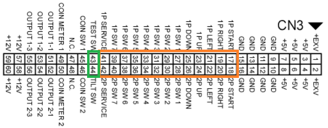
So if you look at the chart and the pinout, there's a correlation. Though the chart shows an example where P1 and P2 have 14 bits. The Type1 I/O does not have a switch 8 for P1 and P2, so let's ignore that one.
The JVS I/O replies to switch commands in bytes or chunks of 8 bits.
Per the chart above, you can see that first row represents byte 1 and includes Test and 3 Tilts. In the case of Type 1 I/O, there is only one tilt switch, so it would likely only report a 1 for one of those values if the tilt switch was activated and report a 0 for the non-existent ones. I don't care about tilt, so I don't have any plans to investigate it further and integrate an actual switch for it. I'll be replying 0 for all tilt bytes. I do, however, want a Test switch to be able to get into the test menu, since my implementation is an I/O replacement in an actual cabinet. Therefore having to go to the back of the cabinet to push a button on the motherboard just to get into the test menu would be a pain.
The 2nd row is byte 2 and includes the first 8 bits of P1 switch data. Since we've got more than 8 bits worth of data, the rest go into byte 3 on the following row.
Then P2 data would be in bytes 4 and 5.
Notice how the columns are labeled starting from the left with bit0. This is the order each bit must be reported to be registered as the associated input. In the first row, according to chart, the Test switch is the left most bit. So in the event that the Test switch is triggered, the reply for byte 1 would be 10000000. When you go to the JVS input test in the test menu and push the test button using the Type 1 I/O, you can see a hex value for the System showing 80. So whenever my designated Test switch is hit, I reply 0x80 (10000000) in the first byte and the motherboard recognizes that the switch has been hit. So that's taken care of.
Now let's move on to P1. In the input test menu P1's bits get shown as a series of hex bytes. The chart aligns with what I'm getting on the input test. 1P Start is the left most bit in the 2nd byte. So if only that switch was triggered the reply for byte 2 would be 10000000 or 0x80.
So now I can get a good sense of the pin order for P1 when assigning pins on the Mega and reporting the inputs to the motherboard:
As I reply to the read switches command, I scan my assigned pins in the order above, building out a reply for the first 8 bits and then a reply for the remaining 5 bits.
Some examples:
If Button 1 and Button 2 are hit the 2 bytes would be:
00000011
00000000
or as seen in the test menu: 0300
If only Button 3 is hit the 2 bytes would be:
00000000
10000000
or as seen in the test menu: 0080
P2 then works the same way in the same order. It's just a matter of assigning them to different pins on the Mega and replying appropriately in bytes 4 and 5.
So now I'm rocking with digital inputs!
 Next up: Coins
Coins are not included as switch inputs. They are managed in a completely separate command and acknowledgement. It looks like the motherboard doesn't even register coin switches. It appears to be up the the I/O board to read those and manage the number of coins, replying with how many coins have been inserted. I briefly tested this with the Type 1 I/O. As I triggered a coin switch, the input test menu incremented a number for the coin row rather than showing it as an on or off switch. I haven't gotten that far into it, but I would guess at some point the I/O would be told to subtract a coin. I'll reply with my findings when I get there.
This also leads me to question what's happening with the coin meters. There are some games that will not boot if a coin meter (or a resistor) is not present. I believe Jambo Safari is an example of this as I have a Naomi 1 and a Jambo Safari cart that will not boot in my cab since one of the meters is removed. I would guess the failure to boot is because for some reason the game is expecting a reply that it isn't getting from the I/O. I will need to make sure my replies for coins indicate that everything is in order, inc
") "The slave that picks up the request sends an ACK back to the master, and pulls it’s output sense to 0." . Se when you are offered a node id, send an empty ack back to master and pull the sense line low. That way the master knows there are no more IO boards on the bus.
"The slave that picks up the request sends an ACK back to the master, and pulls it’s output sense to 0." . Se when you are offered a node id, send an empty ack back to master and pull the sense line low. That way the master knows there are no more IO boards on the bus.


") . Based on poorly translated descriptions, I can't say for sure which of these is typically used for lamp outputs, but Output GPIO 3 seems to be dedicated to ON/OFF bits, so that may be it... I'll likely have to sniff the Type 1 I/O during output tests for a game to verify which one is used.
. Based on poorly translated descriptions, I can't say for sure which of these is typically used for lamp outputs, but Output GPIO 3 seems to be dedicated to ON/OFF bits, so that may be it... I'll likely have to sniff the Type 1 I/O during output tests for a game to verify which one is used.