

hatmoose
Enlightened
After many days of searching I've found some engineering drawings of the TSOP burn-in test socket
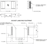

2x HCT244 are for Data Output bus and 3x LVC244A are for Data Input bus?

https://www.mvs-scans.com/misc/toshiba-64mbit-adapter-master-ack2.zip
Just to be clear, they need to be 74HCT244 and not 74HC244
For 64mbit CAPCOM Sony ZN-2 eproms not, but for MVS / Sega Model 3 64mbit eproms yesThese would work as a substitute for any 64mbit mask rom?
2x HCT244 are for Data Output bus and 3x LVC244A are for Data Input bus?
If I understand this well, 3x LVC244A prevent +5V data input from MVS enter to flash rom decreasing it to +3'3V, and 2x HCT244A increase +3'3V data output from flash rom to +5V to the MVS
Also you play how to send Q-15 signal, if by one line of LVC244A for 8-bit input mode, or by one line of HCT244 for 16-bit output mode
So all data are +3.3V output to +5V converted and all address are +5V to +3.3V converted, am I right?The 2x HCT244 are for data (flash to mvs) and the 3x LVC244A are for address (mvs to flash).
The 3 jumpers deal with getting the Q-15 going to/through the correct 244.
1 jumper does the /BYTE signal on the flash
1 jumper picks the trace path from the dip socket pin to HCT244 or LVC244
1 jumper connects the trace from the HCT244 or LVC244 to the flash
correct, the flash should only see 3.3V and the MVS only 5VSo all data are +3.3V output to +5V converted and all address are +5V to +3.3V converted, am I right?
So you can confirm me LVC244 is a +5V to +3.3V level shifter and HCT244 is a +3.3V to +5V level shifter. I have seen in your PCB you establish LVC244 to be active always and HCT244 being active with OE signal state. I supose in my PCBs both HCT244 have to be active LOW because all the data output bus is shared with the 4 flash roms.correct, the flash should only see 3.3V and the MVS only 5V
This shouldn't be a problem if always active in the new implementation I'm making, because the use of the Q0-Q15 of all the 4 roms common bus is going to be OE dependent.The HCT244's are the data lines going from the flash to the MVS. These must only be enabled when the MVS is asking for data from the flash, otherwise it will cause a data bus conflict.
If you want to protect the flash completely, use 3xLVC244 + 2xHCT244 versionSpeaking only for my part, I only tested the version with 5x 74LVC244APW and not the version with mixed with HCT.
You will want something like this if you have the HCT244's between the flash chips data pins and the MVS. The HCT244's won't care that the flash chips aren't outputting anything and will still output a signal if they are enabled. Having no input on the HCT244 is an undefined state so it may output high or low or just randomly flip flop between high/low.The other solution is to install an extra SMD component for detect when all 4 OE signals are HIGH and deactivate the 2xHCT244. A 74LS21 can do the trick: when all 4x OE signals are HIGH, output is HIGH, in other case LOW. That way we can control 2xHCT244 combined activation
So I'll go with 74LS21 implementation. ThanksYou will want something like this if you have the HCT244's between the flash chips data pins and the MVS. The HCT244's won't care that the flash chips aren't outputting anything and will still output a signal if they are enabled. Having no input on the HCT244 is an undefined state so it may output high or low or just randomly flip flop between high/low.


