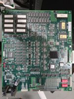
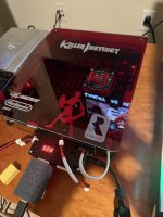
Killer Instinct Dual Board

That method is the only current one until the adapter boards are finished.
I think its a perfectly great way to go.
I am not sure if KI was parched for the KI2 though.
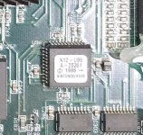
Whats your u96?
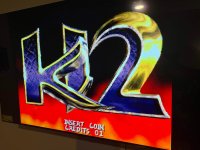
You can dual boot KI2 on a KI board for sure.
 
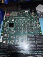
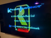
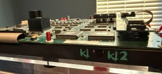
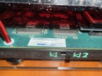
A-20351? If it KI on KI2 can't be done yet I guess I'll just wait it out. Oof. Added cropped pic, compression gods got me on the first one.
 

Attachments

  • 20260302_191920.jpg
    20260302_191920.jpg
    395.7 KB · Views: 29
  • Screenshot_20260309_143748_Photos.jpg
    Screenshot_20260309_143748_Photos.jpg
    274.9 KB · Views: 23
Unfortunately I think until someone figures out a patch its stuck as ki2.
You could get a parts ki1 if you really wanted to use it as a donor for your board.
Or maybe it is dumped.
You would need a 44 pin plcc socket.

Edit: Reviewed the thread. Neko patched ki1 for ki2 board.
There's also a revision of ki1 pcb that is troublesome per the neko github @brandogg.
 
Last edited:
The PCBs didn't make it for the weekend or today, for that matter. It's with the final mile delivery company at least. Maybe tomorrow.
 
Ok, not the end of the world (obviously). I'm just slightly afraid I'd flip the switch while it's running, though I imagine that wouldn't be catastrophic and worse case would corrupt the "HDD".
Nah , nothing bad happens except crashing the game. If you're handy , using a bit more hardware (a relay, a micro controller) and a dual SD card adapter, it's possible hold a button (I used P1 quick kick) during boot to select which game you wish to play.
 
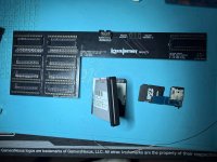
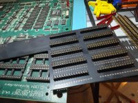
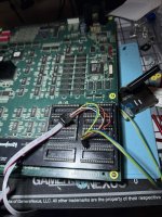
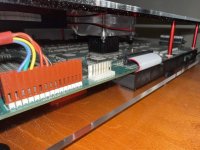
PCBs have arrived. I was worried at first cause I used the intermediary female pin headers, but they had a little too much play and gave me a headache when i saw they didn't align, so I tried flipping regular pin headers upside down just so I could get them to align enough to test. This gives me hope that it might just work. I'll know when I find a way to actually get it in the sockets...lol (and finish soldering).

IMG_7617(1).jpg

IMG_7622(1).jpg
 
Please, everyone, stop using normal 2.54MM headers.
these will over-stress and deform the pins in the socket and make them no longer make good contact with original chips.

In short, if you use these then you'll need to desolder and re-install new sockets if you ever want to go back to the original chips and have the board work reliably.

you need to be using "socket header" pins specifically designed for this. like these:
https://www.amazon.com/dp/B0DR7WVYG7

it's been stated several times in this thread so here's a graphic to help out:
socket_header_warning.jpg
 
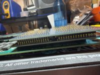
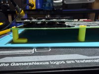
Just an update. I've finished soldering the entire board (that was tooooo many). All the pin headers lined up. I cheated by using another PCB to sandwich the pin headers so they couldn't move and then put them in the DIP sockets on the KI PCB. That forced alignment very nicely. I'll have the final photo of the PCB installed tomorrow with all angles showing it's not buckling. I also programmed all the EEPROMs and images. Last thing I need to figure out is the wiring to the switch cause I want to use the Extension IDC for a cleaner look. I "think" I can carry the 5V and GND through the IDC to their respective pins from the switch location.
 

Attachments

  • IMG_7638.jpg
    IMG_7638.jpg
    182.6 KB · Views: 77
  • IMG_7634.jpg
    IMG_7634.jpg
    276.9 KB · Views: 82
  • IMG_7632.jpg
    IMG_7632.jpg
    178.2 KB · Views: 75
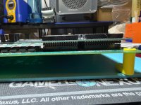
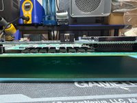
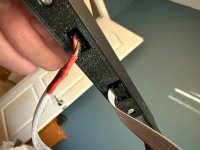
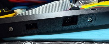
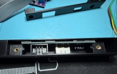
We're in the final stretch. Wiring took a bit as I had to figure out what was already provided and what wasn't and if any wires needed to go to the PCB (the schematics file is either blank or corrupt). If I just installed the switch, you'd have to run 3 wires to the PCB and be done with it, but if you use the EXT, you'll need to run that EXT to a switch and the 3 wires from the microSD adapter. So I did the EXT and made the wiring more complicated cause I didn't want to use the switch pads...lol. I will probably make a PCB (pretty sure I can...only made 2 for myself so far; very primitive) for the switch so you only have to run the IDC cable to the switch area with no additional wires to solder except the 3 coming from the microSD adapter. That's my goal for later. Anyways, as you can see, no buckling in any direction and if fits like a glove. Nervous about putting the ROMs in and testing. lol.
 

Attachments

  • IMG_7643.jpg
    IMG_7643.jpg
    186.6 KB · Views: 69
  • IMG_7644.jpg
    IMG_7644.jpg
    192.5 KB · Views: 62
  • IMG_7645.jpg
    IMG_7645.jpg
    202.8 KB · Views: 60
  • IMG_7647.jpg
    IMG_7647.jpg
    269.9 KB · Views: 65
  • IMG_7648.jpg
    IMG_7648.jpg
    236.3 KB · Views: 60
Please forgive my ignorance, I have read through most of the posts on this topic, but what does this PCB offer over the other methods over dual booting KI/KI2? I don't mean that in any type of negative way, please don't take it that way, I'm just trying to understand because I am extremely interested in doing one of these methods to my KI2. It looks like this acts as an additional socket, except pin 1 (or is it 16?) doesn't connect to the game PCB, and those pins all link together, to U98, and do the switch? Basically it lets you avoid lifting a leg on each ROM and manually connecting them? So then the only wiring needed js from this PCB to the switch (and to the SD switcher), does that seem accurate? Also, will these be available to purchase (as a self-solder kit I assume, if it will be)? Thanks and sorry for the ignorance, I'm a little lost in the sauce trying to take in 33 pages over a couple days.

 
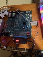
YES! It works! Took me 2 hours to diagnose an issue where it didn't boot when I tested everything. Troubleshooting sites said CF/HDD was not working somewhere (blue screen, bong, pause, reset, repeat). Turns out it was the BOOT ROM. Double check your boot rom before taking it all apart. I am so glad I didn't have to do that. lol. Adapter board is now officially done, almost. I need to edit the PCB to move some sockets down by 1mm. I had to shave 2 sockets a hair to make them sit flat as the solder on a specific row of pins was interfering (it fit okay when it was just the pins and socket but the solder was too much it seems). 1mm will give it the breathing room it needs. I'll post the files after I edit them. I will order another set of 5 to test myself, but I don't want to hold up anyone else. Up to you if you want to wait.
I plan on writing a guide for the full setup on this. The 30+ pages was indeed a lot to go through. Some consolidated instructions, particularly from luke, helped a lot, but still had things I had to figure out elsewhere in this thread.
 

Attachments

  • IMG_7655.jpg
    IMG_7655.jpg
    142.5 KB · Views: 67
  • IMG_7658.jpg
    IMG_7658.jpg
    142.3 KB · Views: 63
  • IMG_7654.jpg
    IMG_7654.jpg
    178.4 KB · Views: 69
Got the files together with the edited 1mm adjustment. I've ordered the PCBs for myself. Gerbers are in here too for simplified ordering if you want to want to try. Here's the updated BOM too. (*Update - was able to add the files after nem's reply about the size limit [also renamed the gerbers file to avoid confusion.] Thank you!).

Part NamePart Number (Digikey)Quantity
32pin socket
2057-ICS-632-T-ND
9
2.54mm round pin headershttps://www.aliexpress.us/item/3256804750241812.html2 (5pcs each).
Should give you enough for
9-16pins and
9-15pins.
3pin header right angle952-2245-ND (only needed if using on-board switch)1
6pos connection header - used for switch extensionhttps://www.aliexpress.us/item/3256805323384920.html
Get 2x3 straight. This is an IDC compliant one.
*Only needed if you want to use the extension switch
**Do not install slide switch if using this method
1
switch slide DPDTEG4367-ND
*I plan on using this switch for the extension as well. Working on a PCB
to simplify the wiring further, but you can use whatever DPDT switch you
want for the extension if you don't want to wait.
1
 

Attachments

Last edited:
I feel like I'm spamming here at this point. lol. I finished the helper PCB and have ordered it. I'm now working on the 3D model for the switch to house the PCB. The existing switch STL is my base. Externally it'll look the same, but inside will be very different.
 
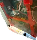
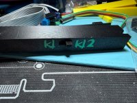
Sorry for the long delay, but it took a while to get the mount right. That CF adapter does not have much room to mount to, but we got it done. I did make a snafu on my helper PCB due to a visual perception and logic issue, but it works regardless. I'll revise and order the new PCBs tomorrow and will post all files and gerbers afterwards. But without further ado, here are some photos of the simplified Multi Board with Switch install.
 

Attachments

  • Switch-CF mount.jpg
    Switch-CF mount.jpg
    105.4 KB · Views: 60
  • IMG_7767(2).jpg
    IMG_7767(2).jpg
    107.6 KB · Views: 56
  • IMG_7766(1).jpg
    IMG_7766(1).jpg
    121.6 KB · Views: 59
  • IMG_7762(2).jpg
    IMG_7762(2).jpg
    158.1 KB · Views: 61
  • IMG_7761(2).jpg
    IMG_7761(2).jpg
    128.4 KB · Views: 65
  • IMG_7759(2).jpg
    IMG_7759(2).jpg
    130.5 KB · Views: 63
  • IMG_7753(2).jpg
    IMG_7753(2).jpg
    137.6 KB · Views: 57
  • IMG_7752(2).jpg
    IMG_7752(2).jpg
    188.6 KB · Views: 62
  • IMG_7751(1).jpg
    IMG_7751(1).jpg
    319.9 KB · Views: 60
Just wanted to update that my new helper PCB came in and works as expected now. Here's what it looks like put together.
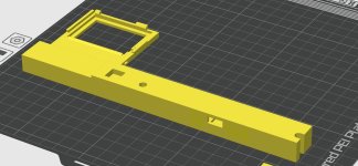
I designed the Spinal print to act as a wire guide. I didn't like the method used in the original case design, so I made my own. Now just waiting on one more PCB that should be here Saturday, I hope, for the final touch before I post everything.
 

Attachments

  • IMG_7890.jpg
    IMG_7890.jpg
    156.6 KB · Views: 58
  • IMG_7892.jpg
    IMG_7892.jpg
    202.5 KB · Views: 60
  • IMG_7893.jpg
    IMG_7893.jpg
    261.9 KB · Views: 56
Back
Top