What's new
Great progress, the part you're going through now is the most fun imo :)

A note on a analog, the way I understand it, the bits reported in the capabilities query is for informationabout resolution to the game only - 16 bits is reported regardless, and probably explains the odd case of 8 bits resolution where 0 bits is reported (if I got that part correctly from the doc - IIRC that is what's reported by the sega IO).

The way it works is you shift/translate your sample up to 16 bits, so that the AD MSB corresponds to the 16 bit reported MSB, in the case of 10 bits, shift it up 6 bits.
Bitwise operators are something I'm going to have to learn a little better. I understand the concepts and how to code for them, but never think about them as a solution.

Thanks for the suggestion!
 
A note on a analog, the way I understand it, the bits reported in the capabilities query is for informationabout resolution to the game only - 16 bits is reported regardless, and probably explains the odd case of 8 bits resolution where 0 bits is reported (if I got that part correctly from the doc - IIRC that is what's reported by the sega IO).
I didn't realize the Type 1 Sega I/O was reporting 0 in the features until just now.

Here's what I've sniffed for its features reply:
0x1: 0x2: 0xD: 0x0:
0x2: 0x2: 0x0: 0x0:
0x3: 0x8: 0x0: 0x0:
0x12: 0x6: 0x0: 0x0:

Translation:
(01) - Digital Switches: 2 Players: 13 bits/Player
(02) - Coin Slots: 2 Slots
(03) - Analog Input: 8 Channels: 0 bits/Channel(?)
(12) - General-purpose Driver: 6 Slots

That's all it shows for features, as far as I can tell, so I can be pretty sure the outputs are going to be driven by one of the 3 GPIO commands as it doesn't look like analog outputs are even a feature of this board. The 6 Slots of GPIO do align with the availability of the 6 outputs on the digital connector for the Type 1.

I'm thinking Type 3 would report having analog outputs as a feature, based on its extra connector, but I wonder if it has any other features on top of a Type 1. I don't have a Type 3 to sniff.
 
I confirmed through sniffing that the lamp outputs are driven by the GPIO Output 1 (32) command, at least in CTHR.

I haven't quite translated that section in the manual to understand the command fully, but it looks like GPIO pins are referred to as "slots" per the features reply, and the write command would then be indicating the state of a given slot. I'll have to dig further into it.

This command and the subtract coins command are going to be two where I need to interpret every part of the command to know how to react. All other commands such as read digital inputs, read coins, and read analog inputs are relatively generic in that the command doesn't vary.

For coin subtraction I need to know which slot and how many to subtract.

For outputs I need to know which slot and which state.
 
Some info on the output command General Purpose Output 1 (32):

In CTHR, when sufficient credits are available in attract mode, the start button flashes on and off.

Here are the 2 forms of the command received:
0x32: 0x1: 0x80
0x32: 0x1: 0x0:

What I can gather from the manual is that the first byte is the command, the 2nd byte says how many bytes worth of data are being sent with GPIO data and the following bytes are the data. I believe it is saying to use the leftmost bit in the data byte as the first driver, so it can be read in order from left to right.

So it appears that once you get into that 3rd byte, basically there's a bit that corresponds to each "slot" of output on your I/O board.

In the case of CTHR, only the start button is being lit.

Here is a pinout with the outputs highlighted. The start lamp is wired to pin 51 - Output 1-1.
JVS Outputs pinout.png


I can probably pretty safely assume that output 1-1 would be the first to be addressed in the data bits. Since we're dealing with only 6 output slots, all of them can be driven within a single byte.

The ON state for the start button is:
(0x80) or 10000000

The OFF state is:
(0x00) or 00000000

So it appears that the left-most bit is dedicated to output 1-1. I can only make assumptions for the rest of them at this point. I don't know if the next one is 2-1 per the pin number order or 1-2 per the player number and order.

In my OR2SP cab, the view change lamp is wired to pin 54 (2-2), so I'll boot that up when I get a chance and try to figure out the order.
 
Here's my follow-up on the output command General Purpose Output 1 (32):

OR2SP is sending out the same command for start and view change lamps. What's interesting about OR2SP compared to CTHR, is that OR2SP is continuously sending out the 32 command, even when it wants the lamps to stay off. I'd have to double check, but I think CTHR is only sending it when it wants the start lamp on and then again when it wants it off. In the event that it's staying off, I think it doesn't send a command. I could be wrong about that, though.

Anyway, the command for the view change lamp ON is:
0x32: 0x1: 0x8

That translates to:
00001000

So the left most bit is the start button at the first pin on the connector. The view change lamp is the 5th bit from the right. It appears to be following the player order per the pinout lables and not the pin order.

So I believe these are the bits, starting from the left, that correspond to each output on the Type 1:
Bit 1: Output 1-1 - Pin 51
Bit 2: Output 1-2 - Pin 53
Bit 3: Output 1-3 - Pin 55

Bit 4: Output 2-1 - Pin 52

Bit 5: Output 2-2 - Pin 54

Bit 6: Output 2-3 - Pin 56


In the event that both lamps are on, the command is:

0x32: 0x1: 0x88


So, using that information, I can now reference wiring diagrams and get an idea for the various lamps in a given game and reroute them to my cabinet's lamps as part of my per game configuration.
 
On another note: I'm likely going to migrate over to the Arduino Due.

The major factors that would make the Due preferable to the Mega 2560 is that it uses micro USB ports and it has 2 of them. 1 for programming and standard Arduino serial interface over USB and the other for native USB, such as making it act as a USB controller for the PC.

The Mega 2560 has a single standard Type B port, the same one that the JVS connector uses, so there's a risk of accidentally plugging into the wrong port. In the event of trying to use the board as a native USB device, things get a little more complicated due to having to flash the firmware of the USB driver chip, which isn't very straight forward, and you have to flash it back to get your standard programming functionality back.

The Due has the same footprint and pinout, so all work that I've done up to this point is transferable.

So I can continue with the main goal of having a replacement I/O, and I think that will remain pretty compatible with the Mega 2560, but once I get into the USB functionality, I think that may end up being pretty exclusive to the Due.

The prices for the cheapo clones aren't too different to make the cost be a consideration.

The Mega 2560 clone is about $12 and the Due clone is about $18-$26. It's weird, I bought a Due for $18 at the beginning of this week on Amazon and now the listing shows $26...
 
(03) - Analog Input: 8 Channels: 0 bits/Channel(?)
0 - means unknown,
its also worth mention - document you are reading now is about JVS 3 rev 1.3, however all real world JVS IO I know is older JVS 2 rev 1.1, so they lack number of features (mostly that ones written using red color in PDF)
if I not mistaken - prior to latest jvs rev 3 there was no 'bits per channel' field, and you see there just 0.
 
(03) - Analog Input: 8 Channels: 0 bits/Channel(?)
0 - means unknown,its also worth mention - document you are reading now is about JVS 3 rev 1.3, however all real world JVS IO I know is older JVS 2 rev 1.1, so they lack number of features (mostly that ones written using red color in PDF)
if I not mistaken - prior to latest jvs rev 3 there was no 'bits per channel' field, and you see there just 0.
Thanks for the input!

I did notice the JVS revision 2 reported by the type 1 I/O, but wasn't sure of the implications.

Any idea, for games that have I/O requirements, are those restrictions based on the features reply or other information as well?
 
not sure games have some specific requirements regarding JVS protocol revisions, they are just not use newer features.
 
I spent some frustrating hours today trying to figure out why my board kept failing when booting a game, vs working fine when just booting with no game, and I think it was mostly due to trying to debug with the Arduino while it's acting as a JVS I/O. In this case the Arduino is managing JVS communication over one serial port and sending debug messages over another. I think I was running into issues for some of the larger commands from the master, like where it sends the main board ID with what I guess is information about the game booted, where I was in the middle of writing out a debug message and the JVS communication got underflowed, making everything fail... So I cut out a lot of my debugging in that area and can now successfully get my I/O working in games!

So the thing that has me really confused now is coin management. I thought it was going to be as simple as telling the main board how many coins are inserted and then get a command back from the main board to subtract one. As far as I can tell, though, I'm never getting a subtract command. In OR2SP, I noticed it booted up showing something like 7 credits that I had entered on a previous session with a different I/O, so I know my board wasn't telling it how many coins there were... I kind of think now that the game is managing coins and really it's just looking for an increase in coin count from the I/O in order to increase credits.

Another frustration is trying to get this migrated to the Arduino Due. The issue may be 3.3v ttl vs the Mega's 5v. I'm not entirely sure if my RS-485 module is 3.3v compatible so I may be running into issues transmitting with the Due.
so they lack number of features (mostly that ones written using red color in PDF)
Do you have a copy of this you can post? The version I have is all black and white, so I'm not sure what you're referring to.
 
Last edited:
I spent some frustrating hours today trying to figure out why my board kept failing when booting a gave, vs working fine when just booting with no game, and I think it was mostly due to trying to debug with the Arduino while it's acting as a JVS I/O. In this case the Arduino is managing JVS communication over one serial port and sending debug messages over another. I think I was running into issues for some of the larger commands from the master, like where it sends the main board ID with what I guess is information about the game booted, where I was in the middle of writing out a debug message and the JVS communication got underflowed, making everything fail... So I cut out a lot of my debugging in that area and can now successfully get my I/O working in games!

So the thing that has me really confused now is coin management. I thought it was going to be as simple as telling the main board how many coins are inserted and then get a command back from the main board to subtract one. As far as I can tell, though, I'm never getting a subtract command. In OR2SP, I noticed it booted up showing something like 7 credits that I had entered on a previous session with a different I/O, so I know my board wasn't telling it how many coins there were... I kind of think now that the game is managing coins and really it's just looking for an increase in coin count from the I/O in order to increase credits.

Another frustration is trying to get this migrated to the Arduino Due. The issue may be 3.3v ttl vs the Mega's 5v. I'm not entirely sure if my RS-485 module is 3.3v compatible so I may be running into issues transmitting with the Due.
so they lack number of features (mostly that ones written using red color in PDF)
Do you have a copy of this you can post? The version I have is all black and white, so I'm not sure what you're referring to.

Good news that you got it working in games!! Any video you can show?

generally going from 5v to 3.3v is pretty straight forward. 3.3v will still be recognized as a binary 1 in a 5V system, so you just need to make sure that you power the PCB with 3.3V.
 
Good news that you got it working in games!! Any video you can show?
I don't actually have the cabinet inputs wired up yet. I destroyed my previous custom PCB and will have to revisit the design since I think I had the JVS port routed incorrectly.

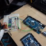
I don't even have the necessary controls wired up at this point to play anything, so there's nothing worth showing except maybe some spaghetti on a breadboard:
IMG_20160923_151118.jpg
 
generally going from 5v to 3.3v is pretty straight forward. 3.3v will still be recognized as a binary 1 in a 5V system, so you just need to make sure that you power the PCB with 3.3V.
I'm going to have to investigate this further. I did attempt it with the RS485 module's VCC powered by 3.3v out from the Due board, but still don't think I'm transmitting successfully. I don't know if the failure is at the transmitter enable pins (DE/RE on the module) or the voltage of the TX port on the Due.

I THINK I can rule out faulty wires as all I did was transfer the wires from the Mega to the same pins on the Due, and everything works with the Mega. TTL voltage is the only difference I can figure might be causing the issue.

Edit:

I'm pretty sure I'm using the same RS-485 module used in the TeensyJVS project. The Teensy has 3.3v TTL, so now I'm confused about whether or not that's the issue. In the schematic they have for TeensyJVS I notice they're powering the module with 5V, which I was doing in my original attempt without success.
 
Last edited:
I have a PCB design together that takes into the account my more recent breadboard discoveries, specifically with regards to handling the sense line, so hopefully I'll be successful the next time. I also discovered that my original board didn't have the the USB Type B pinout incorrect... It was the JVS manual that had the pinout listed incorrectly, making me think I had it wrong. At this point I'm not even sure what was wrong in the original board I put together, but for sure the software had issues that were keeping things from working.

Anyway, with 2 blanks left, I went to cut my latest design on my CNC machine and realized I had screwed something up and messed up the first one... and tried to get fancy on the 2nd one putting both the drilling and carving into the same process, and screwed it up during the manual tool change from the drill bit to the v-bit... So I basically burned through 15 blanks for this project so far. I've learned a lot though, and should have a better outcome with the next order of blanks. It was less than $10 worth of blanks, and I had more than $10 worth of fun! :thumbsup:

Some remaining goals are:
1. Get a freakin' custom PCB cut and put together successfully.
2. Work on code for interpreting the Write GPIO 1 command so that I can output to the correct lamps.
3. Configure software to work with all inputs from my OR2SP cabinet.
4. Work on code for dynamic configuration.
5. Figure out what's going on with the Arduino Due and migrate to it.
6. Work on code for native USB output from the Arduino Due to use the cabinet as a PC controller.
 
Good progress! And if it only costed you $10 of blanks, I'm tempted to do it as well :)

I'm preparing my setup to read out all the responses from my JVS cards so you can add them to your device :thumbsup:
 
Back
Top